
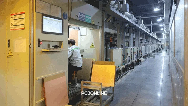
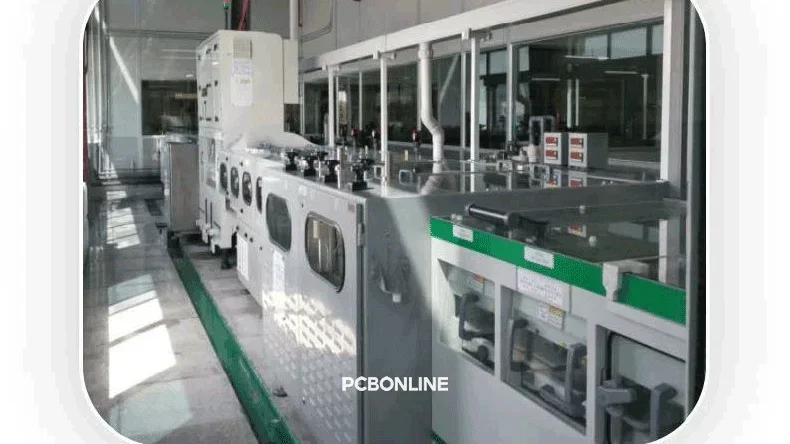
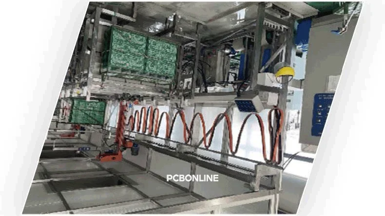
VCP plating line at PCBONLINE's PCB factory
PCBONLINE is a one-stop printed circuit board (PCB) manufacturer for mid and high-end applications. Our two manufacturing bases in Jiangxi and Jiangsu Provinces provide mass production of advanced circuit board fabrication, including HDI PCBs.
How can we provide advanced PCB manufacturing and ensure its quality and efficiency? Besides 26 years of experience, our PCB factory has complete PCB fabrication equipment and inspection laboratories, which contribute to our capabilities in independently completing the PCB manufacturing process.
Check the PCB fabrication equipment and inspection labs at PCBONLINE's PCB factory.
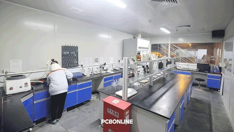
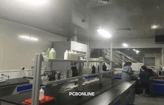
Chemistry and Physics Laboratories
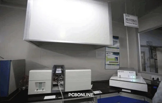
First, at PCBONLINE's advanced PCB factory, let's view the two labs for measuring the chemical and physical performances of PCBs.
- ICP-OES (inductively coupled plasma optical emission spectrometry): Analyzes metal ion concentration (Cu, Ni, Fe) in plating solution, etching solution, or wastewater.
- UV-Vis spectrophotometer: Measures organic compounds, such as developers and stripping agents, and solution concentrations.
- ICP-MS/OES: Ensures compliance with RoHS/EPA regulations for wastewater discharge.
- Mercury analyzer: Detects whether there are Hg ions in the PCB wastewater.
- pH/ORP/conductivity meters: Monitors wastewater treatment processes.
- TOC analyzer (total organic carbon): Measures organic pollution in wastewater.
- Acetone wipe test: Qualitatively checks resin curing.
- Fume hoods: Handles corrosive acids (HNO₃, HCl) and solvents.
- Explosion-proof refrigerator: Stores flammable chemicals like developers.
- Waste liquid collection system: Segregates spent acids, heavy metal waste, and organics.
Our chemistry laboratory is equipped with comprehensive chemical analyses. With this chemistry lab, PCBONLINE has the certification to buy, use, and store gold salt for gold plating and immersion gold in PCB fabrication, and the capability to treat the wastewater after gold plating and immersion gold.
Now, let's have a glance at the physics lab at PCBONLINE's PCB factory. In the physics lab, you will find:
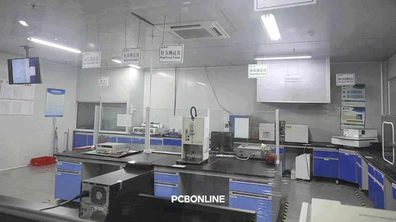
- A high-voltage insulation tester. This device checks the electrical insulation properties of PCBs.
- A resistance tester is also present. It measures the electrical resistance of circuits.
- A peel force tester evaluates the adhesion strength of copper traces.
- An impedance tester measures the characteristic impedance of transmission lines on the PCB.
- The RoHS tester is a critical piece of equipment. It ensures compliance with the Restriction of Hazardous Substances directive.
- Soldering ovens are used for thermal reliability testing.
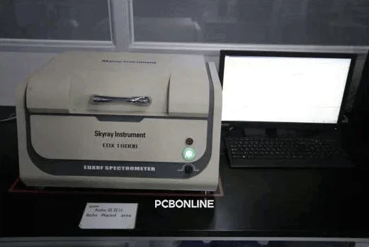
- An AAS atomic absorption spectrophotometer analyzes the elemental composition of materials.
- A plating layer THK tester measures the thickness of plated layers.
With the complete testers and other equipment in our laboratories, we can prepare the solvents for and after the PCB manufacturing process, and ensure the reliability and performance of our PCBs and PCBAs after manufacturing.
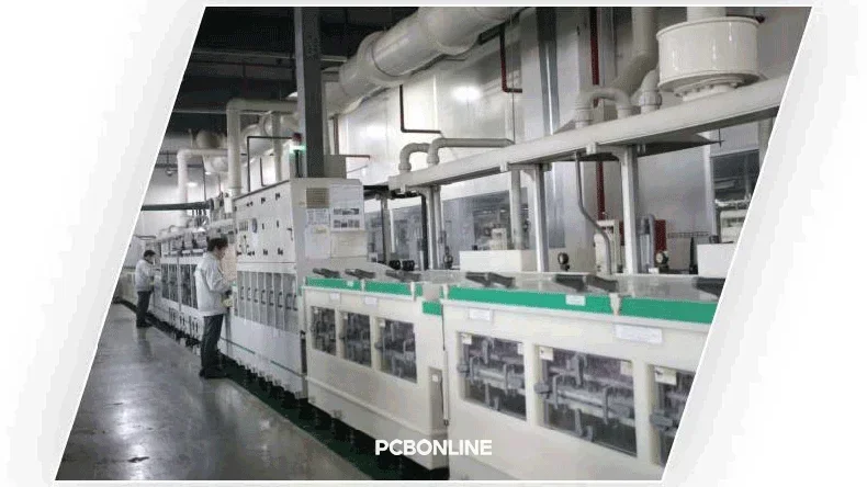
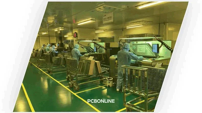
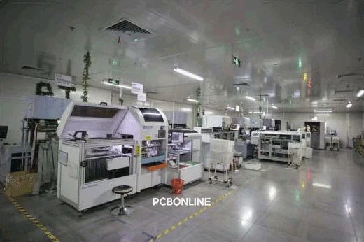
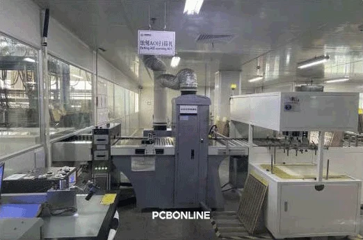
PCB Manufacturing Equipment at PCBONLINE's PCB Factory
PCBONLINE's PCB factory is equipped with comprehensive equipment for every possible step in PCB manufacturing. For the complete PCB manufacturing process, for example, you can read our HDI PCB manufacturing process in a previous blog.
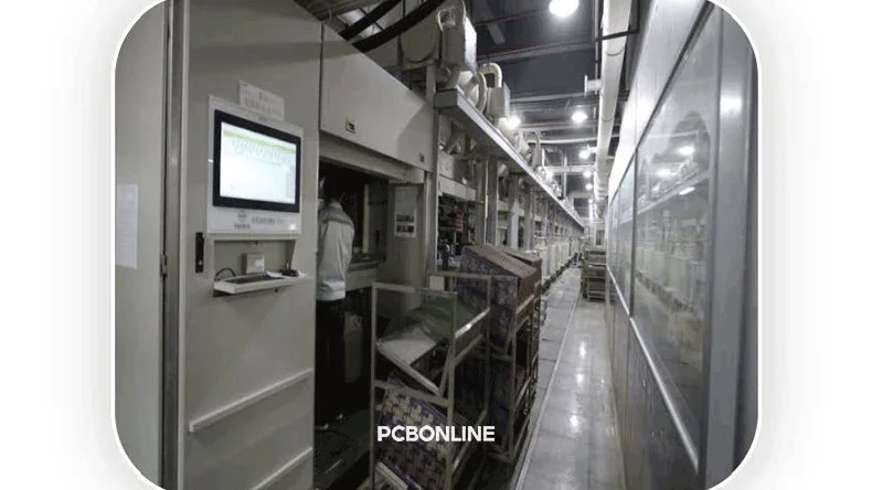
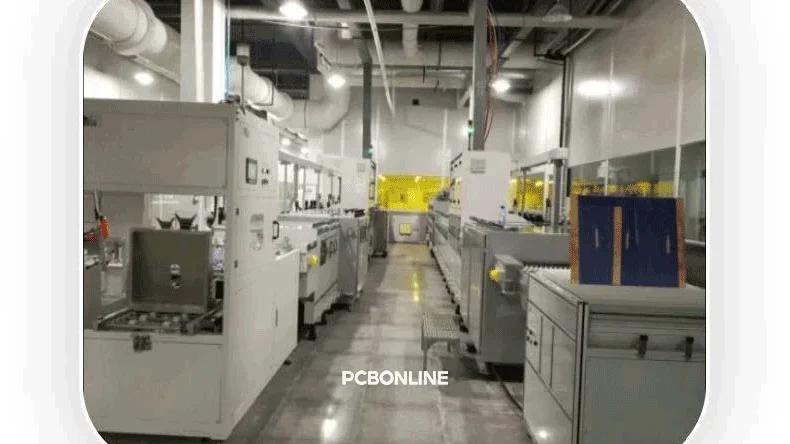
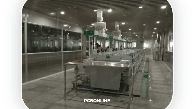
There is too much equipment in our PCB factory to list all of it in this article. So we only show part of the PCB production equipment at PCBONLINE's PCB factory.
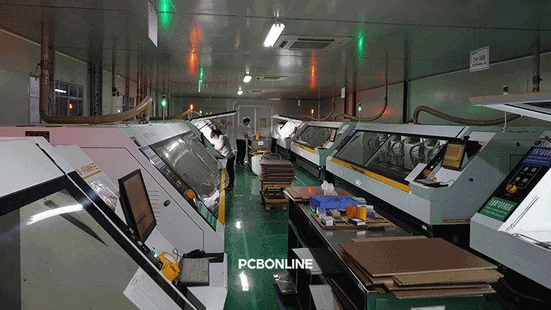
High-precision drilling machines: Mechanically drill holes in the PCB substrate for component placement and interconnections.
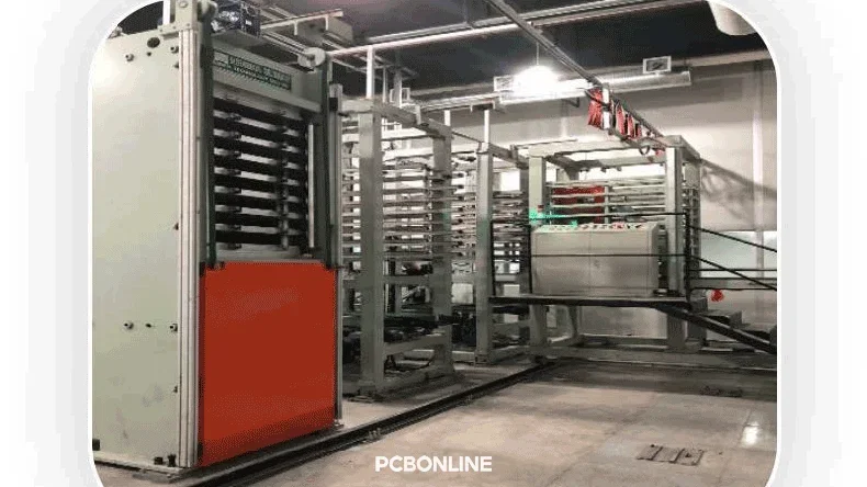
Lamination machine: Layers of substrate, prepreg, and copper foil are pressed together under high temperature and pressure. It creates a solid and unified board.
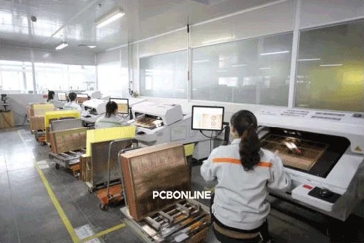
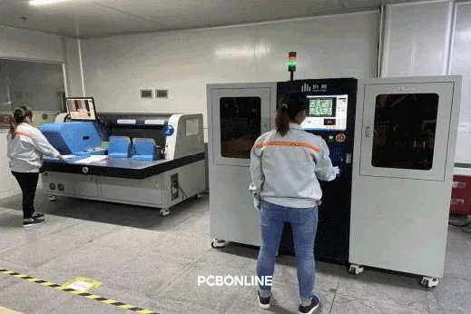
Vertical Continuous Plating (VCP) system: The VCP technology provides uniform copper plating. It enhances the conductivity and durability of the circuits. It is a more advanced method compared to traditional horizontal plating. Advanced PCBs like flexible PCBs and HDI PCBs all require VCP copper plating.
Pre-treatment and post-treatment machines: circuitry. They clean and prepare the copper surfaces to ensure optimal adhesion for the photoresist.
Outer Surface Plating (OSP) line: OSP is a surface finish application. The OSP line applies an organic protective layer onto the PCB copper pads. It protects the copper from oxidation. It also ensures good solderability.
Solder mask pre-treatment line: It prepares the PCB surface for the solder mask application. The solder mask protects the circuit traces from oxidation and prevents solder bridges during assembly.
S.E.S. (soldermask exposure system) line: It is used for precise solder mask imaging. This system ensures accurate application of the solder mask pattern.
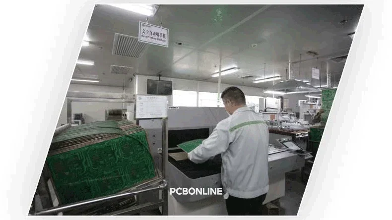
Silkscreen printing line: This production line employs marking and labeling on the PCBs, including component designators, logos, and other identifying information. Our automated silk screen printing line further enhances efficiency. It applies legends and other markings with high speed and accuracy.
CNC (computer numerical control) machines: They are used for precise routing and shaping of the PCB. The CNC machine cuts the PCB panel board to its final dimensions and creates any necessary cutouts or slots.
Immersion gold plating line: It is used for applying the immersion gold surface finish on PCBs, like flexible PCBs. The immersion gold line applies a nickel layer and then a gold layer onto the copper pads. Gold provides excellent conductivity and corrosion resistance. It is often used for high-reliability applications.
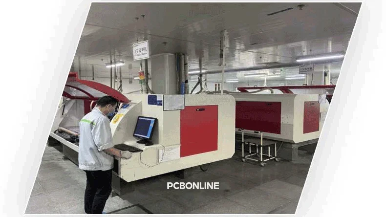
CCD (charge-coupled device) and LDI (laser direct imaging) exposure machines: They use lasers to directly image the circuit patterns onto the photoresist. They offer higher resolution and accuracy compared to traditional film-based methods. For fine-line PCBs such as HDI PCBs, the CCD LDI machine is necessary, and that's why the advanced PCB manufacturer PCBONLINE's PCB factory is equipped with them.
PCBONLINE's commitment to high-quality PCB manufacturing is evident in our advanced production and testing equipment. With these production machines, plus our rich experience in manufacturing and quality management, we ensure high precision and efficiency throughout the PCB manufacturing process.
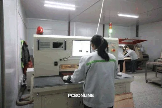
Testing and Inspection Equipment for Quality Control
Quality assurance is paramount at PCBONLINE. Our PCB factory is equipped with comprehensive testing and inspection equipment to ensure the functionality and reliability of every PCB produced.
Below are part of the testing and inspection machines we use during and after PCB fabrication.
Test machines: They are used to check for opens and shorts in the circuit. They ensure proper connectivity.
The chemistry and physics laboratories: As mentioned earlier, the chemistry laboratory and physics laboratory also serve as testing facilities. They perform various material and performance tests.
Online AOI (automated optical inspection) machines: An AOI machine is integrated into the production line. AOI machines use cameras to scan the PCB for defects after each circuit layer is generated after etching. The AOI machine ensures high quality and reduces human error.
VRS (visual review system): A VRS is used for detailed visual inspection. It allows the operator to magnify and examine specific areas of the PCB. It helps to identify subtle defects that might be missed by automated systems.
Plating layer thickness tester: It measures the thickness of various plating layers in the PCB. It ensures proper electrical performance and durability.
X-ray inspection machine: It provides non-destructive inspection to reveal hidden defects within the PCB layers. With the X-ray inspection, we can check out issues with internal connections or voids in solder joints.
AVI (automated visual inspection) system: It is another automated inspection. Similar to AOI, an AVI machine uses vision systems to identify defects.
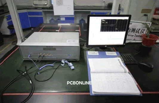
Impedance tester: Impedance control is essential for high-speed digital designs to ensure signal integrity. An impedance tester verifies that the characteristic impedance of transmission lines is within specified tolerances.
RoHS tester: It is used for environmental compliance. It verifies that the materials used in the PCB are free from restricted hazardous substances.
PCBONLINE: Your Reliable Source Factory PCB Manufacturer
If you are looking for reliable and high-quality PCB manufacturing services, you can partner with the one-stop PCB manufacturer PCBONLINE. Whether you need advanced PCB prototypes or mass production, PCBONLINE can meet your custom demands.
Founded in 1999, PCBONLINE has two large advanced PCB manufacturing bases, one PCB assembly factory, stable supply chains, and an R&D team. We have successfully worked on many PCB and PCBA projects in all walks of industries.
PCBONLINE manufactures all types of PCBs. The PCBs we provide include flexible PCBs, HDI PCBs, high-frequency PCBs, ceramic PCBs, thick-copper PCBs, aluminum PCBs, copper-core PCBs, rigid-flex PCBs, transparent PCBs, and glass PCBs.
We have powerful PCB manufacturing capabilities and can complete the PCB manufacturing and assembly processes independently.
As a source factory manufacturer for PCBs, PCBAs, and box-build assemblies, PCBONLINE offers cost-effective electronics manufacturing.
We save your money, efforts, and time to help your project smoothly turn into real products.
Our engineers have rich experience in R&D and engineering, and we can do the R&D or assist your development and optimize your design.
With comprehensive testing and inspections, we offer high-quality PCB manufacturing certified with ISO 9001:2015, ISO 14001:2015, IATF 16949:2016, REACH, RoHS, UL, and IPC-A-600 Class 2/3.
When your PCB or PCBA project goes into the mass production stage, we will refund the fees for R&D and prototypes and offer free PCBA functional testing.
PCBONLINE has successfully worked on many PCB and PCBA projects for terminal companies, solution companies, research institutes, and business makers around the globe. Our professional design for manufacturing (DFM) will pave the way for your project's success. If you want to get a quote or ask questions, you can send emails to info@pcbonline.com.
Conclusion
PCBONLINE's advanced PCB factory with cutting-edge equipment for independent PCB manufacturing and comprehensive quality control ensures the PCB quality and production efficiency. If you need advanced PCBs or have any questions, you can contact PCBONLINE by email or from the table on the right.
PCB fabrication at PCBONLINE.pdf


