
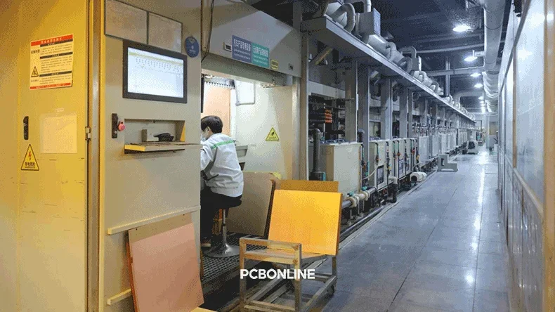
VCP plating line at the HDI PCB supplier PCBONLINE
PCBONLINE stands out as a top high-density interconnect (HDI) PCB supplier. We offer high-quality HDI PCB manufacturing and assembly and ensure successful electronics manufacturing for your project. This article will detail the HDI PCB manufacturing process, equipment, and capabilities of the HDI PCB supplier, PCBONLINE.
HDI PCB Supplier PCBONLINE's Capabilities
First, let's explore the manufacturing capabilities of the HDI PCB supplier.
PCBONLINE operates HDI PCB manufacturing and assembly across our manufacturing infrastructures — two advanced PCB manufacturing bases and one PCB assembly factory. We provide custom HDI PCB design and manufacturing services, including varying copper thicknesses.
|
Features
|
HDI PCB supplier capabilities
|
|
Daily capacity for HDI PCBs
|
3000m²
|
|
Rigid-flex HDI PCB layer
|
4-24
|
|
Rigid HDI PCB layer
|
4-64
|
|
HDI PCB thickness
|
0.15mm to 3.2mm
|
|
High-density layer quantity
|
Up to 20
|
|
HDI PCB stackup
|
1+N+1, 2+N+2, 3+N+3, 4+N+4
|
|
Microvia types
|
Blind, buried, staggered, stacked, and skipped
|
|
Min. laser drill diameter
|
0.075mm
|
|
Min. mechanical drill diameter
|
0.15mm
|
|
Varying copper thickness
|
100μm to 125μm
|
|
Solderability standard
|
>95% (IPC-TM-650 2.4.14)
|
|
Surface finishes
|
OSP
|
|
HASL: SMD 40µ to 2000µ", GND 30µ to 800µ"
|
|
|
ENIG: Au 1µ to 5µ", Ni 80µ to 200µ"
|
|
|
Immersion tin: 0.8µm to 1.2µm
|
|
|
Immersion silver: 0.15µm to 0.45µm
|
|
|
Hard gold plating: Au 1µ to 50µ", Ni 80µ to 200µ"
|
|
|
Peelable mask: 5mil
|
|
|
Carbon ink: 0.3mil
|
|
|
Applications
|
Battery switches, power distributors, motor controls, LED applications
control, automotive, satellite, microsystems, and industrial technology, communications electronics
|
HDI PCB Manufacturing Process at PCBONLINE
PCBONLINE is equipped with complete production lines and machines to complete the HDI PCB manufacturing process. Our commitment to HDI PCB supply lies in professional and accurate HDI PCB manufacturing.
Our HDI PCB manufacturing process involves multiple stages — inner layer processing, drilling and hole preparation, outer layer processing, solder mask and silkscreen, plating and surface treatment, final fabrication and testing, testing and quality control, and material and performance analysis.
Inner Layer Processing
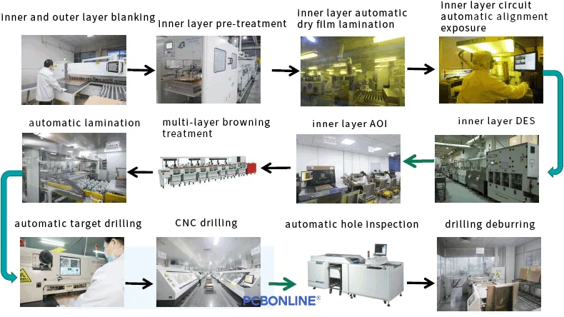
Inner and outer layer automatic blanking: The process starts with automatic blanking of both inner and outer layers. This ensures precise sizing of the base material.
Inner layer pre-treatment: Next, the inner layers undergo automatic pre-treatment. This prepares the surface for subsequent steps, ensuring optimal adhesion and cleanliness.
Inner layer automatic dry film lamination: An automatic dry film lamination process is then applied to the inner layers. This dry film acts as a resist during imaging.
Inner layer circuit automatic alignment exposure: The circuit patterns are precisely aligned and exposed onto the inner layers automatically. This step uses advanced imaging technology.
Inner layer DES: The inner layers then proceed to the DES (Develop, Etch, Strip) line. This process removes unwanted resist and etches the copper, defining the circuit traces.
Inner layer AOI: Automated Optical Inspection (AOI) is performed on the inner layers. This is a crucial inspection step, detecting any defects in the circuit patterns.
Multi-layer browning treatment: A multi-layer browning treatment is applied using an automatic line. This enhances adhesion between layers and improves reliability.
Automatic lamination: Multiple layers are automatically laminated together. This creates the multi-layer structure of the HDI PCB.
Drilling and Hole Preparation
Automatic target drilling: Automatic target drilling is performed. This ensures accurate drilling locations.
CNC drilling: Computer Numerical Control (CNC) drilling machines are used. These machines provide high precision and repeatability.
Automatic hole inspection: An automatic hole inspection machine verifies the drilled holes. This ensures proper hole quality and dimensions.
Drilling deburring: After drilling, a deburring process removes any rough edges. This prepares the holes for subsequent plating.
Automatic desmear and PTH (plating through hole): Holes are then desmeared and undergo Plating Through Hole (PTH). This process creates conductive pathways between layers.
Outer Layer Processing
Outer layer pre-treatment: Outer layers receive a pre-treatment, preparing their surface for further processing.
Outer layer automatic dry film lamination: Similar to inner layers, outer layers have dry film automatically laminated. This protects areas not to be etched.
Outer layer circuit fully automatic alignment exposure: The outer layer circuit patterns are exposed with full automatic alignment. This ensures precise pattern transfer.
Outer layer circuit development: The outer layer circuits are developed.
VCP automatic electroplating: A Vertical Continuous Plating (VCP) automatic electroplating line is then used. This provides uniform and high-quality plating.
Automatic electroplating: An automatic electroplating line is utilized. This deposits metal onto the PCB surface.
Outer layer automatic film removal, etching, and tin removal: An automatic line handles film removal, etching, and tin removal for the outer layers. This reveals the final circuit patterns.
Outer layer etching online AOI: An online AOI inspection machine inspects the outer layer etching. This real-time inspection identifies any etching defects.
Outer layer AOI mid-inspection: Another AOI mid-inspection is conducted on the outer layers. This ensures the quality of the etched patterns.
Sandblasting and grinding: A sandblasting and grinding machine is used.
Solder Mask and Silkscreen
Solder mask connected screen printing: Solder mask is applied in a connected screen printing workshop. This protects the circuit traces from oxidation.
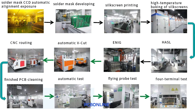
Solder mask CCD automatic alignment exposure: The solder mask is exposed using CCD automatic alignment. This ensures precise alignment of the solder mask openings.
Solder mask developing: The solder mask is then developed. This reveals the areas to be soldered.
Silkscreen printing: Silkscreen legends are printed. This provides component identification and other markings.
High-temperature baking of silkscreens: The printed silkscreens undergo high-temperature baking. This cures the ink and ensures durability.
Plating and Surface Treatment
Hot air solder leveling (HASL) pre- and post-treatment: A pre- and post-treatment line for hot air solder leveling (HASL) is available. This process provides a tin-lead finish.
ENIG (electroless nickel immersion gold): Our capabilities include Electroless Nickel Immersion Gold (ENIG) surface finish. This finish offers excellent solderability and long-term reliability.
Final Fabrication and Testing
Automatic V-Cut: Automatic V-CUT machines are employed. This process partially cuts the boards for easy separation.
CNC routing: Computer Numerical Control (CNC) machines are used for routing. This precisely cuts the individual PCBs from the panel.
Finished PCB cleaning: Finished PCBs are cleaned in a dedicated workshop. This removes any debris or contaminants.
Testing and Quality Control at PCBONLINE
Automatic test: Performs various electrical tests.
Flying probe test: A flying probe test is available. Flying probe testers can test complex and high-density boards efficiently.
Four-terminal test: A four-terminal tester is used for precise resistance measurements. The four-terminal test ensures the integrity of the electrical connections.
Finished PCB dehumidification and leveling equipment: Dehumidification and leveling equipment are used for finished PCBs. This ensures the boards are flat and moisture-free.
Automatic AVI inspection for finished PCBs: Automated Visual Inspection (AVI) is performed on finished PCBs. This system automatically detects visual defects.
FQC (final quality control): Final Quality Control (FQC) is conducted as a comprehensive inspection before packaging.
FQA (final quality assurance): Final Quality Assurance (FQA) is the last step in quality verification, ensuring all specifications are met.
Material and Performance Analysis

Full-size measurement: Full-size measurements are taken. This verifies the overall dimensions of the PCB.
Metallographic section observation: Metallographic sections are observed under a microscope. This allows for detailed inspection of internal structures.
RoHS testing: RoHS (Restriction of Hazardous Substances) testing is conducted. This ensures compliance with environmental regulations. We have a dedicated RoHS tester.
Impedance measurement: Impedance is carefully measured. This is crucial for high-speed signal integrity.
Gold, nickel, tin, and REACH testing: Testing for gold, nickel, tin, and REACH compliance is performed. This ensures material composition meets international standards.
Ionic contamination testing: Ionic contamination testing is conducted. This identifies any corrosive residues on the board.
Withstand voltage test: A withstand voltage test is performed. This verifies the dielectric strength of the PCB.
Packaging: The final products are packaged.
Finished boards are cleaned thoroughly. They undergo dehumidification and leveling. This prepares them for inspection and packaging.
Laboratories and Equipment at the HDI PCB Supplier PCBONLINE
The HDI PCB supplier PCBONLINE has two laboratories for chemical and physical analysis and comprehensive testing equipment.
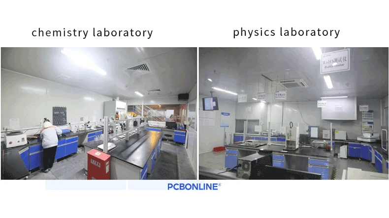
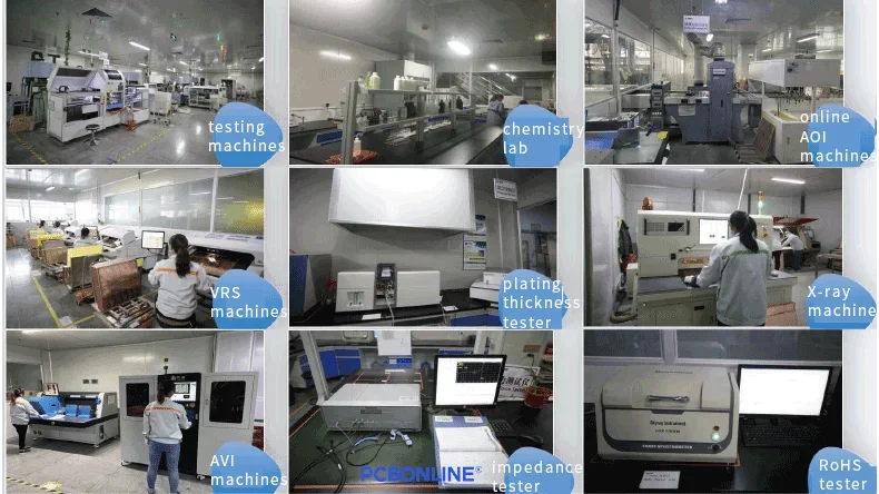
- Chemical laboratory: We have a well-equipped chemical laboratory. This supports process control and material analysis.
- Physical laboratory: Our physical laboratory is used for various physical performance inspections, such as mechanical and thermal testing.
As an HDI PCB supplier that completes the manufacturing process independently, our factory is equipped with all the PCB production lines and machines.

- Drilling machines: Drill the PCB holes mechanically.
- VCP machines: Vertical Continuous Plating (VCP) machines are part of our setup.
- Circuit pre- and post-treatment lines: We have dedicated lines for pre- and post-treatment of circuits.
- Lamination machines: Our facility includes modern lamination presses.
- OSP line: Organic Solderability Preservative (OSP) lines are used for surface finish.
- Solder mask pre-treatment equipment: We use specialized equipment for solder mask pre-treatment.
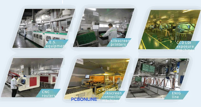
- S.E.S. equipment: Our factory includes S.E.S. (Strip, Etch, Strip) equipment.
- Silkscreen printers: We use character inkjet printers for silkscreen.
- CCD LDI exposure machines: CCD LDI (Laser Direct Imaging) exposure machines are utilized to offer high precision for imaging.
- CNC routers: Automatically route the PCB panel board to the required dimensions.
- Automated silkscreen connection machines: Apply the silkscreen assist lines to help link component labels to their actual positions, improving readability and reducing assembly errors.
- ENIG line: Apply a nickel layer and then a gold layer on the PCB copper pads as the ENIG surface finish.
- Testing machines: Conduct various electrical tests.
- Online AOI machines: Our online AOI systems provide continuous inspection during production.
- VRS (visual repair system): VRS helps in repairing detected defects.
- Plating thickness tester: A plating thickness tester ensures correct plating levels.
- X-ray inspection machines: X-ray inspection is used for internal layer inspection.
- AVI (automated visual inspection): AVI systems automatically inspect for visual defects.
- Impedance testers: Impedance testers verify signal integrity.
- RoHS testers: RoHS testers ensure environmental compliance.
One-Stop HDI PCB supplier from R&D to Fabrication and Assembly
If you plan to develop an HDI PCB or PCBA project and need a turnkey PCB supplier with R&D capabilities to ensure the success of your project, you can partner with the HDI PCB and PCBA supplier PCBONLINE.
Founded in 2005, PCBONLINE has two advanced PCB manufacturing bases, one PCB assembly factory, stable supply chains, and an R&D team.
PCBONLINE has strong HDI PCB fabrication capabilities, including FR4 HDI PCBs from 4 to 64 layers, HDI flexible PCBs up to 8 layers, HDI rigid-flex PCBs from 4 to 24 layers, and HDI high-frequency PCBs from 4 to 24 layers.
PCBONLINE can meet your HDI PCB demands from the initial idea to high-volume production.
Minimum laser drill: 0.075mm, minimum mechanical drill: 0.15mm
We can make HDI PCBs with structures of 100 µm and 125 µm.
Microvias can be made as single microvias, staggered vias, stacked vias, and skipped vias.
High-density circuit layers up to 20, and microvia PCB layer up to 64.
HDI PCBs 1+N+1, 2+N+2, 3+N+3, and 4+N+4 can be manufactured, and microvias can be in any layer in R&D.
PCBONLINE pays attention to quality and cost-effectiveness in HDI and microvia PCBs. Our engineers with more than 20 years of experience will provide you with one-on-one engineering support throughout the project. If you want to get a quote or ask questions, you can send emails to info@pcbonline.com.
Conclusion
The one-stop HDI PCB supplier PCBONLINE is equipped with cutting-edge equipment and comprehensive quality control to pave the way for your HDI project's success. If you need HDI PCBs or have any questions, you can contact PCBONLINE by email or fill out the form on the right.
PCB fabrication at PCBONLINE.pdf


