
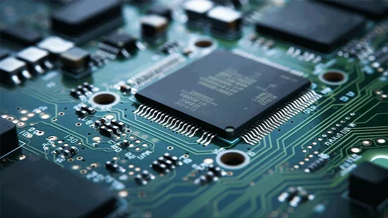
Understanding printed circuit assembly, including the differences between PCA and PCB, the costs involved, and the detailed assembly process, is essential for effective communication with your electronics hardware supplier about PCBA manufacturing.
A PCA project can encounter many issues and risks. A key to your PCA project's success is the engineering support from your PCA manufacturer.
In this blog, you can see three exciting PCA projects to understand what a PCA manufacturer can do to help the PCA R&D and manufacturing. You can also about all the details of PCA, and you won't feel puzzled when putting your design into production!
PCA vs PCB
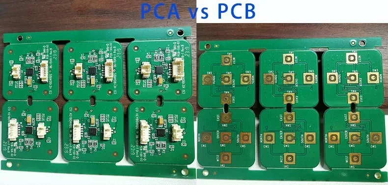
First, let's understand what PCA and PCB, respectively. PCA (Printed Circuit Assembly) and PCB (Printed Circuit Board) are two terms used in the production of electronic devices.
A PCB is a board using conductive pathways, or traces, etched from copper sheets laminated onto a non-conductive substrate. It mechanically supports and electrically connects electronic components and is the foundation upon which electronic components are mounted and interconnected.
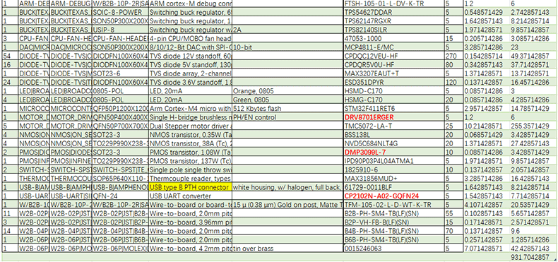
A PCA is known as a PCBA. Its assembly process involves SMT (surface mount technology) and PTH (plated-through hole technology). SMDs (surface-mount devices) are placed on the PCB and soldered by reflow. Through-hole components are inserted through the PTH holes with their leads and solder by the wave or selective soldering process.
From the above, you can understand that PCB and PCA are different stages in electronics manufacturing, and the PCA process follows PCB fabrication. Below, you can see a straightforward table of PCA vs PCB.
|
PCB
|
PCA
|
|
A blank board without components
|
A functional board fully assembled with components
|
|
The PCB fabrication process involves cutting laminate, etching the copper laminates, drilling, plating, and lamination.
|
The PCA process includes SMT assembly and PTH assembly, including placing and reflow soldering SMDs and inserting leads and wave soldering PTH components.
|
|
PCB serves as the backbone of copper traces and thermal conductivity. Its copper pads and PTH holes are designed for assembling components.
|
PCA is a functional electronic board that can be used in electronic devices. It is used as the working component in the electronic device after assembly.
|
Project Examples of Printed Circuit Assembly
A PCA manufacturer is not only a contract manufacturer. It can also provide design for manufacturing (DFM) to solve technical issues and improve your design so that you won't suffer from potential risks and economic losses due to design defects.
Below, you can see three PCA project examples where PCBONLINEoffers solutions to solve technical issues for our clients.
PCA No.1 - High-current circuit design and manufacturing
Project background: The project is designed to be used in testing equipment for an electric vehicle (EV) battery pack. One of the controller boards requires high currents of 100V DC up to 180 amps. The hardware engineer on the client side meets challenges during PCB design and asks for our engineering support.
Technical issues to solve:
1. How to enable the PCB to load high currents of 100V DC up to 180 amps.
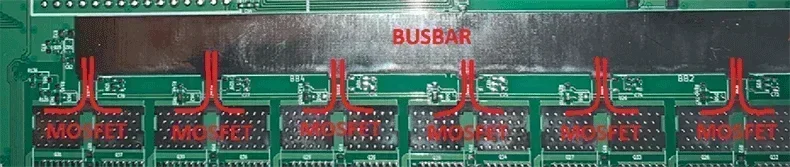
2. How to transfer currents from the copper bus to SMT components and then back to the copper bus (as shown in the figure below).
The engineers at PCBONLINE have rich experience in high-current PCB design and manufacturing. We empower the client's hardware design from the R&D phase and provide many feasible solutions in structure and thermal management design. Through our engineering support, we accelerate the clients's R&D process and push forward the smooth batch production of the products.
Once we received the support request from our client, we responded quickly and came up with the below design suggestions and solutions:
- We suggest our client use copper busbars to replace the copper foil design of the PCB.
- We calculate the thickness, width, and package design of the copper busbars according to the schematic diagram and provide the CAD drawings for our client's reference.
- We accurately calculate the copper busbar size to facilitate PCB SMT assembly, improve production efficiency, and reduce defective rate (if the copper busbar size is too large, it will deform under high temperatures during wave soldering).
- We suggest our customer use MOSFETs in multiple network designs to shunt voltage (MOSFETt of special sizes can be customized according to the application scenario to realize two different module networks of high voltage and low voltage).
Following our engineers' suggestions, the client completes the PCB design smoothly, and after PCBONLINE finishes the prototype, it validates the success of the sample. Now, we have put the design into bulk production.
In the early stage of the R&D process, PCBONLINE offers free technical support, which saves the R&D costs and time for our client.
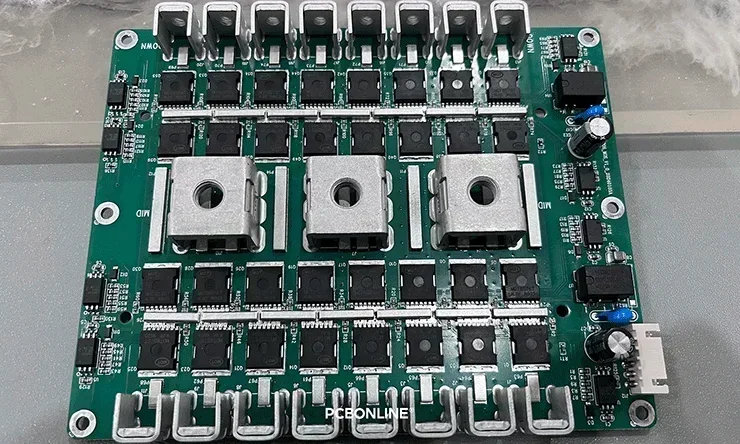
The final PCA is shown below.
PCA No.2 - One-stop design and manufacturing of high-brightness LED lights
Project background: The client is a well-known German swimming pool lighting and heating pump manufacturer. They entrust us with developing a high-power, high-lumen swimming pool light.
Challenges to solve:
1. The brightness needs to reach 10,000 lumens at 100W power.
2. As the LED light is installed underwater, the corrosion resistance, safety, and waterproof requirements of the PCB board must be considered.
3. Within the limited size, RGBW 4 colors of the LED light are designed, and the lightwave, color temperature, and light color of each color are of strict requirements. The client's PCA acceptance standard is the industrial grade.
In this PCA project, PCBONLINE has technical advantages in the thermal management of metal substrate PCBs and aluminum nitride PCBs. We jointly developed this project with our LED chip supplier and provided our client with two products for different scenarios. The one-stop original design manufacturing service we provide to our client is as follows.
Product AFor product A, we select the 6W/(m·K) aluminum plate with a high thermal conductivity as the heat dissipation substrate.
In circuit design, we adopt a thermal and electrical separation design. As shown in the figure below, the heat generated by the LED is directly conducted to the aluminum substrate through the solder pad at the bottom. There is no dielectric layer in the middle. Meanwhile, the power supply circuit and the heat dissipation circuit are separated, which perfectly solves the heat dissipation problem.
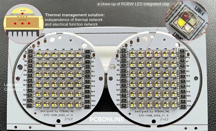
Regarding the LEDs, we customize the LED chips as the brightness required to reach 10,000 lumens at 100W power. The brand of the light-emitting chips we select is "SANAN." We package the LED chips to achieve the light parameters required by our client.
What are the pros and cons of this product?
The advantage of this solution is its low production cost. However, the disadvantage is that the aluminum substrate has poor corrosion resistance, and the light from the LED beads is not uniform enough. It is suitable for low-end market applications, so we helped the client develop the product B.
Product BFor product B, considering that the product is used in environments with high humidity, we select aluminum nitride as the PCB substrate for its excellent corrosion resistance.
Another advantage of using aluminum nitride as the PCB substrate is its excellent thermal conductivity of ≥170 W/(m·K).
We use the COB technology to replace SMD LED beads to ensure the uniformity of light.
Besides, we even add the light dimming system to the PCB board to realize and control the communication with the motherboard.
The PCA is below.
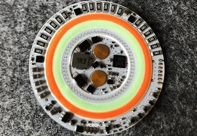
Though this solution has a high production cost, its overall performance, safety, and optical parameter realization effect far exceed product A. It is suitable for high-end markets, such as hotels, gymnasiums, etc.
PCBONLINE contracted all aspects of this high-lumen LED underwater light project from R&D to PCBA production testing.
When the project proceeds to the bulky production stage, PCBONLINE refunds the R&D expenses at the early stage to our customer.
The R&D expenses for all batch production PCA projects by PCBONLINE will be returned after the product is successfully mass-produced. Our R&D team serves to develop mass-produced products.
Through this cooperation, where we help to complete the R&D in the early stage, PCBONLINE wins recognition and also more orders from our client.
PCA No.3 - IoT motherboard cost reduction
Project background: Our client commissioned us to produce an IOT motherboard for a shared scooter
PCBONLINE did not participate in the early research and development of this project, but we helped our client solve technical problems during the free DFM process before production, avoiding the cost caused by the client's design defects and helping the client reduce at least 10% of the component procurement cost.
During the pre-production DFM process, our engineers found that the shielding cover designed by the client was a patch-covering type, which would cause the components under the shielding cover to be unable to process AOI and X-ray inspection after SMT was completed. So we suggested that the client change to a snap-on shielding cover, which can be covered after AOI and X-RAY are completed, and the client agreed to our suggestion.
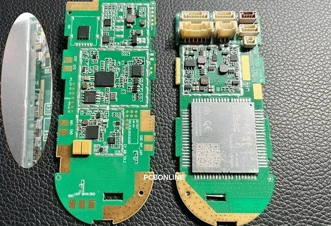
During the DFM check before production, our engineers found that the BOM (bill of material) specification descriptions of three models of passive components were different from the pad packages of the PCB design. We reminded our client to check this problem, and the client finally modified the PCB pad and circuit design to solve this potential risk.
Besides, as PCBONLINE integrates different BOMs to purchase components, the component brand and agents give us great price discounts, especially for the communication modules of IOT products (such as Espressif, SIMCOM, and Neoway, and we have strategic cooperation with the original manufacturer). We have a great price advantage, and our client told us that they saved 15% of the component procurement cost.
Costs of PCA Printed Circuit Assembly
In most printed circuit assembly projects, SMT components account for about 80% of the component cost, but the SMT assembly cost accounts for only 60%; through-hole components account for about 20%, but the PTH assembly cost accounts for 40%.
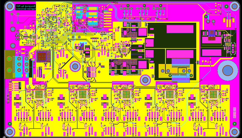
For example, you can see a quotation for a fine-pitch PCB assembly project made by PCBONLINE. From the below PCB Gerber image, you can see that the PTH components are in small quantities, and the SMDs are in large quantities for each PCA.
Below is the BOM (bill of materials or component list) of the example PCA project. Each PCA has only 1USB type B PTH connector that is highlighted and 5total for the project, and all the others are SMDs. But since there are PTH components that need PTH assembly, we need to turn on both an SMT line and a PTH line.
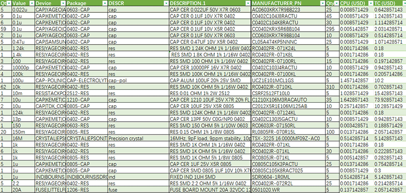
What is the cost for this 5-piece PCA prototype project? It's $1423.41in total. Sounds high? Let's break it.
The components cost $931.70, the assembly costs $328.57, the 5 PCBs cost $25.714 x 5 = $128.57, and the freight costs $46. There's a $ 11.43 discount, so the total PCA fee (including PCBs, components, and assembly) is $1423.41.
As this PCA requires 0.05mm fine-pitch assembly and requires both SMT and PTH technologies, the assembly fee of $ 328.57 is very competitive, and PCBONLINE's PCB assembly services are quite affordable. If it requires only SMT assembly, there's no need to turn on the PTH line for wave soldering, and the assembly fee can be lower.
For this PCA project, PCBONLINE also provides:
- SMT stencils
- Design for manufacturing (DFM)
- Design for testing (DFT)
- Design for assembly (DFA)
- Comprehensive PCA tests such as functional testing
They are all included in the above PCA assembly fee.
SMT and PTH for PCA Printed Circuit Assembly
A printed circuit assembly process can contain both SMT and PTH assembly. It can also require only SMT assembly or PTH assembly. Using PCA technology depends on the device's requirements.
In recent years, SMT has been preferred for many PCA projects by engineers. SMT has the following advantages:
- Fully automated production, thus suitable for PCA bulk production
- SMDs feature compact design and easy mounting
- SMT features fine pitch. Even the smallest SMDs with the footprint 01005 can be precisely mounted.
However, the disadvantage of SMT is that the component adhesion on the PCB is not as good as PTH. PTH has these characteristics:
- Has strong mechanical strength and can withstand large external forces
- PTH components have a larger size than their corresponding SMDs and are suitable for high-power circuits that need a wider clearance and creepage distance.
Components used in industrial control, inverters, and other high-current applications are usually high-power components, such as connectors. PCAs for high-current devices must meet the needs of transmitting high voltage and high current. Therefore, sufficient electrical clearance (the shortest air distance between two conductive parts) and creepage distance (the shortest path along the surface of an insulating solder mask bridge between two conductive parts) must be considered during PCB design, and these factors affect the size of the components. Thus, PTH components are required for high-power PCA.
Besides, operational convenience and the mechanical strength of the components are important factors. For example, the connector is usually the interface for the PCB to communicate with the external devices so it may encounter many external forces. Components assembled with through-hole technology are much more reliable than corresponding SMDs. Whether it is strong pulling, squeezing, or thermal shock, the PTH component can withstand it and is not easy to detach from the PCB.
What is the PCA Process
Below are the steps of a PCA process that involves SMT assembly and PTH assembly and their brief explanation.
1. Solder paste application
At first, the PCBs loaded in the loader are sent one by one automatically into the solder paste printing machine, in which an SMT stencil is pre-set. Solder paste is applied to the PCB through the stencil, which ensures that paste is deposited accurately and sufficiently on the pads where components will be mounted.
2. Solder paste inspection (SPI)
The solder paste on the PCB is scanned and inspected to ensure its position, thickness, and size are qualified for soldering.
3. Pick and place
Two SMT machines (high-speed and functional SMT machines) pick SMDs from tapes and reels and place them on the designated pads.
4. X-ray inspection
![]()
For HDI PCBs and any of these SMDs, an X-ray inspection before reflow soldering is needed: BGA(ball grid array), NTC (negative temperature coefficient) thermistors, QFN (quad flat no-lead) ICs, LGA (land grid array), and flip-chip ICs.
The PCB is exposed to X-rays, which penetrate the PCB and components to image the internal structures.
5. Reflow soldering
The PCB with placed SMDs passes through a reflow oven, which pre-heats and bakes the board, melting the solder paste, forming the IMC (intermetallic compound), and cooling down the board to create solid solder joints.
6. AOI
After reflow soldering, the PCB with placed components is soldered to be a PCA. It is automatically sent to pass through an in-line AOI (automated optical inspection) machine, which inspects the solder joints and components to ensure accuracy and PCA quality. Each AOI process is equipped with a specialized quality control technician, who will also visually check each PCA.
7. PTH component insertion
The leads of the PTH components are manually or half-automatically inserted through the PTH holes.
8. Wave soldering or selective soldering
PTH components are soldered by wave soldering or selective soldering. Wave soldering requires a custom jig to expose only the PTH holes. The wave soldering machines preheat the PCA and soak the PCA into waves of molten solder, which solders the leads to the PTH copper walls.
Selective soldering doesn't require a jig and solders the PTH component leads to the PTH walls by spurring molten solder onto the PTH holes one by one. It prevents thermal shock to thermal-sensitive components on the PCA.
10. PCA cleaning and trimming
After wave soldering or selective soldering, the PTH components leads on the other side of the PCA is trimmed to about 0.25mm. Next, the PCA is cleaned with water-based cleaning agents and then ionized water or ultrasound to remove the flux residue and other contaminates from the PCA.
11. Value-added in post-assembly stage
In the post-assembly stage, there's a series of value-added processes for the PCA, including:
- Functional testingto ensure the PCA works
- Conformal coatingto spray a protective coating to further protect the PCA from thermal shock, vibrations, dust, chemicals, and humidity and extend the service life of the PCA
- IC burn-in programmingto transfer a program into the IC so that it can control the PCA as designated
- Thermal agingto ensure the PCA's reliability for long-term operation
- Box-build assembly, including the enclosure manufacturing, final product assembly, and application simulation testing to deliver the final electronic devices
- Labeling, packaging, and shipping according to your requirements
The above steps give you an overall understanding of the printed circuit assembly process. With a clear step-by-step explanation of the PCA process, you can communicate with your PCBA manufacturer without many doubts now. But hold on, you can know more details of printed circuit assembly below.
Details of Printed Circuit Assembly
There are many to consider in a PCA project. Learning as many details of printed circuit assembly as possible will help you think comprehensively about your project during design, lower the risk of electronics manufacturing failures, and communicate with your PCA manufacturer effectively.
1. Double-sided PCB requires two times of SMT assemblies. To reduce the possibility of oxidation of the SMDs on the first side, you can choose nitrogen reflow or vacuum reflow.
2. The main components of solder paste are alloy powder and flux. The common solder paste alloy composition is Sn/Ag/Cu305 alloy in the ratio of 96.5%/3.0%/0.5% with a melting point of 217°C. If your PCB material, such as PET, has a low melting point, the solder paste should have a higher silver ratio for reflow soldering at lower temperatures.
3. Thick-copper PCBsor boards with a large area of PCB busbars dissipate thermal faster, so their PCA reflow soldering requires higher temperatures.
4. After printed circuit assembly, the PCB warpages should be within 0.75%of its diagonal.
5. SMT stencil openings are generally 4umsmaller than PCB pads to prevent solder ball defects.
6. After unpacking, if the humidity instructor card says the humidity is greater than 30%, it means that the IC is damp and absorbs moisture.
7. Improper preheating and cooling during reflow soldering can cause issues like solder paste collapse, solder balls, solder creepage, unwetting, head-in-pillow, tombstoning, and voids on the PCA.
Knowing these details, you can get more insight into printed circuit assembly and work with your PCA supplier more efficiently.
High-quality One-stop PCA Manufacturer PCBONLINE
To turn your PCB and electronic device design into real products, you can work with PCBONLINE for high-quality and affordable printed circuit assembly at one stop.
Founded in 1999, PCBONLINE has two large advanced PCB manufacturing bases, one PCB assembly factory, stable supply chains, and an R&D team to provide you with turnaround printed circuit assembly and electronic manufacturing services. Regarding the molds and enclosures for electronic manufacturing, PCBONLINE provides them by having long-term cooperation with the top 3 mold and enclosure factories in China.
Powerful printed circuit assembly capabilities and rich experience to meet all requirements and solve technical issues in your PCA project.
You can turn your design into reality under one roof, from PCB fabrication, component sourcing, PCA manufacturing, value-added processes, and box-build assembly from prototypes to bulk production.
Relying on the EMS PCB assembly factory, PCBONLINE can source original components from component factories and first-level suppliers that have been audited at lower prices.
Manufacturing for the entire printed circuit board assembly project is traceable, including components, PCB materials, molds, enclosures, machines, operation specs, faculty, time, and shipping.
High-quality printed circuit assembly certified with ISO 9001:2015, IATF 16949, RoHS, REACH, UL, and IPC-A-610 Class 2/3.
Affordable printed circuit assembly and electronics manufacturing as PCBONLINE is a PCA source factory manufacturer.
PCBONLINE has many successful printed circuit assembly experiences to share with various industries, including industrial, automotive, commercial, computer, communication, medical, aerospace, and defense electronics. If you want to know our PCA experience in your industry, or if you feel interested in getting a quote for your PCA project, please email info@pcbonline.com. The professionals at PCBONLINE will provide one-on-one engineering support throughout your project.
Conclusion
In electronic industries, you will eventually need printed circuit boards after you design a project. Manually soldering components onto a small number of boards with big footprints can work for DIY devices. However, for devices for commercial, industrial, automotive, and even aerospace and military uses, you will need printed circuit assembly, which provides precision and reliability and doesn't have to be expensive. The knowledge of printed circuit assembly will help you turn your design into production smoothly and confidently. PCBONLINE provides one-stop and high-quality PCA manufacturing, and it is cost-effective to have PCA manufacturing from prototypes to bulk production. Don't hesitate to get in touch with PCBONLINE or chat with us from the online chat window.
PCB assembly at PCBONLINE.pdf


