

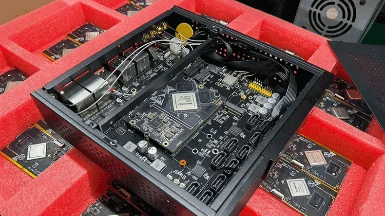
Design for Manufacturability, or DFM, is the engineering review that checks whether a PCB design can be built reliably and at a reasonable cost on the manufacturer's own equipment.
On a PCBA project, DFM covers the bare PCB and the assembly together.
Trace widths the etching line can hold. Drill sizes the drilling process can maintain. Footprints the pick-and-place machines can work with. A BOM the supply chain can source.
Most articles about PCBA DFM read like rulebooks. Keep annular rings above 0.15mm. Space your components at least half a millimeter apart. Put fiducials in three corners. The rules are correct, and your CAD tool checks most of them before you export.
What those articles never explain is what your manufacturer does with your files after you hit send on the inquiry.
This article covers that part. What gets reviewed in the first 24 hours after your Gerber and BOM arrive, and how a good DFM review can cut your manufacturing cost before you have even seen a quote.
What PCBA DFM covers
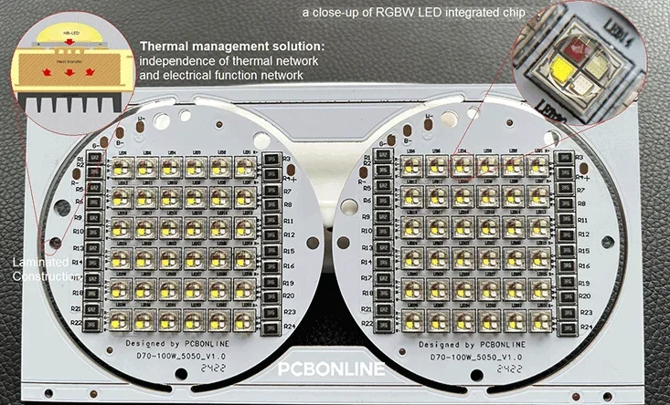
A PCBA project has three production stages, and DFM applies to all of them.
Fabrication DFM
The fabrication review checks the bare PCB against the factory's process window: trace and space, drill sizes, annular rings, impedance stack-ups, soldermask slivers, copper balance across layers.
If a design has a 0.075mm trace next to a 0.09mm gap, and the factory's etching process holds 0.075/0.075mm, the review flags it before any material is cut.
Assembly DFM
The assembly review checks the layout against the SMT line. Footprint geometry against the component package, component spacing against nozzle clearance, panel design against the conveyor width, test point access against the ICT fixture.
A design can pass every fabrication rule and still cause tombstoned resistors at reflow, because two pads on a passive component have unequal thermal mass.
Box build DFM
The box build review checks the assembled PCBA against the final product. Connector clearance against the enclosure, cable routing against the EMI gasket, screw boss locations against component height zones.
Assembly houses that stop DFM at the reflow oven miss this entire layer.
At PCBONLINE, one engineering team runs all three reviews. We are a one-stop PCBA manufacturer, so the same people who review your Gerber also see the PCB come off the SMT line and go into the enclosure.
Feedback from production flows straight back into the next DFM review, instead of dying in an email thread between three vendors.
The first 24 hours: what we check when your files arrive
When an inquiry arrives with Gerber files, a BOM, and assembly drawings, the review starts immediately. Three questions get answered before any quote is issued.
Does the PCB fit our manufacturing capability?
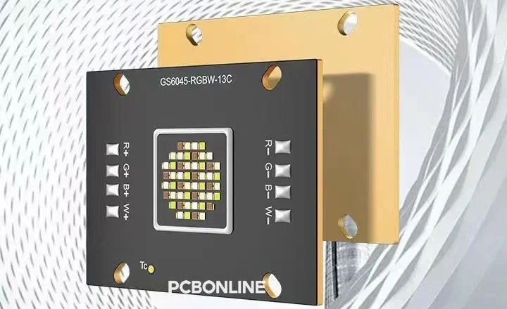
We are a mid-to-high-end PCB manufacturer with an attached assembly factory, so our process window is wide.
Standard multilayer PCBs, HDI builds with microvias, high-frequency materials, rigid-flex, aluminum and copper substrates, thick copper, ceramic substrates: designs across this range are routine work for us. For most inquiries, the answer is yes.
Some designs sit outside what anyone in the industry can build.
One recent example: a customer needed a complex, high-precision circuit on a transparent flexible PCB. Transparent substrate materials support basic circuit patterns, but the feature density and layer count this design required exceed what the material can carry. No factory can build it as drawn.
For transparent-flex designs like this, the usual fix is to split the circuit. The high-density section moves to a standard polyimide flex PCB. The section that needs transparency stays on the transparent material. A connector joins the two.
The customer keeps the intended function and gets a manufacturable product.
If a design needs this kind of restructuring, we tell you before quoting, with concrete suggestions. That is the entire point of an early review.
Redesigning at the inquiry stage costs days. Redesigning after a failed prototype run costs weeks and the prototype money.
Does the Gerber match the BOM?
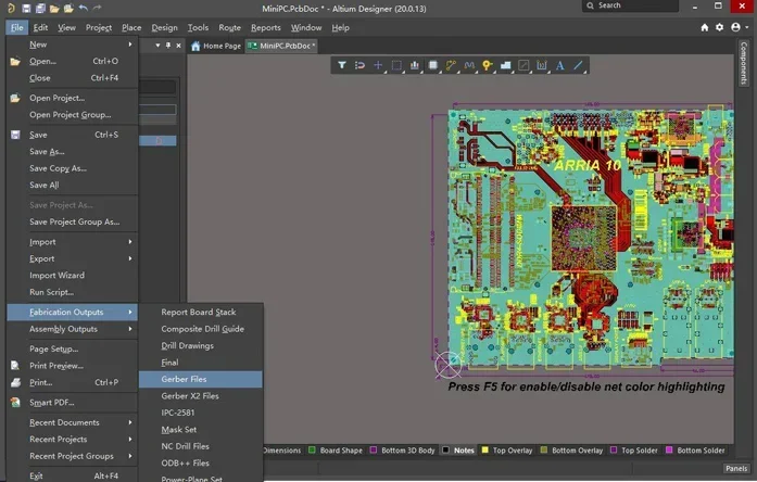
The second check cross-references the two files against each other. The most common finding is a footprint that does not match its BOM line.
The layout has a 0402 footprint, and the BOM specifies a 0603 part for that reference designator. Or a connector footprint was copied from a different part in the same family with a different pin pitch.
These mismatches are silent killers. A 0603 capacitor will sometimes sit on an 0402 footprint and pass visual inspection, then fail in the field after thermal cycling.
The machine places what the BOM says, onto the copper that the Gerber draws. The gap between the two only shows up as intermittent defects.
The review also checks that every component on the BOM has a reference designator on the PCB, and that every designator on the PCB has a BOM line.
A missing decoupling capacitor is a functional bug. A BOM line with no footprint stops the pick-and-place program from generating at all.
Can every part be sourced?
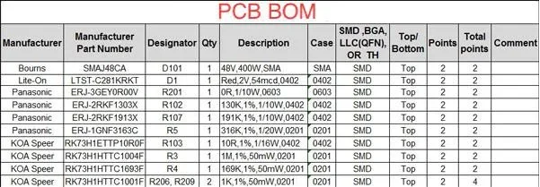
The third check runs the BOM against component availability. Parts go end-of-life without warning. Distributors go out of stock on popular microcontrollers for months at a time.
Some parts on your BOM may be available only from brokers, with the counterfeit risk that implies.
When a part looks risky, we check alternates before quoting. Same function, same package, different manufacturer, available in volume.
If an alternate needs a footprint change, the review catches it here. At this stage, the change costs one edit in your CAD tool. After production starts, it costs a stencil remake and a component reorder.
Once these three checks are done, you receive a quote with a firm lead time within 24 hours of the inquiry.
The 24-hour figure is itself a quality signal: it is only possible when the review is real. A quote produced in an hour means nobody opened the files.
Cost-saving suggestions before you commit
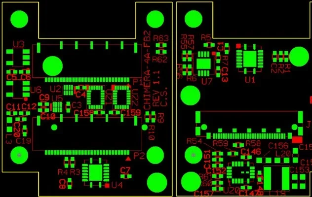
Capability checks and file checks protect you from failure. The next layer of DFM does something different: it reduces what you pay.
When our engineering team reviews a layout and sees a way to cut manufacturing cost without touching function or reliability, we bring it to you before quoting, with the expected savings attached.
Examples from real projects:
Panelization
A PCB dimensioned at 168mm × 118mm fits a standard 210mm × 297mm production panel once, with 30% of the panel wasted. Adjusting the outline by a few millimeters, when your enclosure allows it, fits two per panel and cuts the fabrication cost nearly in half.
Layer count
A 6-layer stack-up where two planes carry almost no signal can sometimes drop to 4 layers and still hit the same impedance targets. 4-layer PCBs cost less per square meter.
Material selection
High-frequency laminates cost several times more than standard FR-4. Some designs specify them out of habit, when the signal rise times do not require them.
The reverse also happens: an impedance-critical design on standard FR-4 that needs the controlled-Dk material to hit its targets.
None of these are suggestions you are obliged to take. You know your product constraints better than any manufacturer does. Our position is that you should hear the option and the number before you commit, not after.
The customer's goal is a product that sells, and a product that sells is built at a cost the market supports. We work toward that as a partner, not as a factory chasing the next order.
DFM does not end at the quote
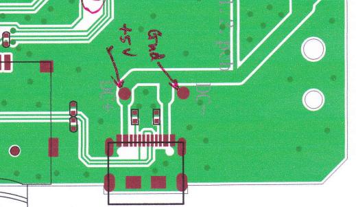
The review before quoting is the visible part. The real advantage of DFM at a one-stop manufacturer is that it continues through every stage, from prototype to volume production.
During fabrication, the CAM engineer checks each production file against the process on the floor.
At SMT assembly, first article inspection verifies each component value against the BOM before the run continues.
At box build, the fit of the PCBA into its enclosure is checked against the drawings.
When any stage surfaces an issue, the correction lands in the project file, and the next revision of the design starts from a clean baseline.
This is also why prototype and volume should stay with one manufacturer. The DFM feedback loop only works when the people who learned from your prototype are the people running your production.
Split the two across vendors, and every lesson from the prototype phase has to be relearned at volume.
When there is no design yet
Some customers arrive with a validated design and need it built. Others arrive earlier.
You have your own engineering team
Our engineers join the project at the early design stage and work through the layout with your people. They choose component packages that stay available in volume, design test access for the ICT fixture, and lay out the panel before the outline is frozen.
A design that goes through this process reaches the prototype stage ready to build, with the DFM review reduced to confirmation instead of correction.
You have no R&D team
We evaluate the requirement first. If it is within reach of our engineering capability, our R&D department delivers the complete design and takes it through manufacturing.
You get a working product and a production partner in the same engagement, with no design house between you and the factory adding margin and losing detail.
What to look for in a DFM partner
A manufacturer's DFM process tells you what kind of supplier you are dealing with. A real one is easy to spot.
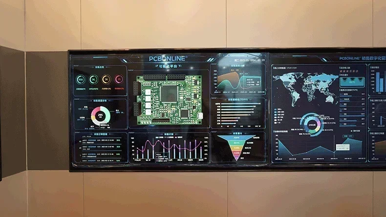
The quote arrives with flags attached.
Warnings about footprint mismatches, risky parts, and cost-saving options in the same message as the price. A bare number with no engineering commentary means the files were priced, not reviewed.
The review happens before money changes hands.
Every serious manufacturer checks files before production starts, because defects at reflow are the factory's problem. The ones who check before quoting are treating your cost as their problem too.
The same team sees the project through.
Fabrication, assembly, and box build under one engineering review, so problems get fixed once instead of forwarded.
This is not a test you run on every board. It is a qualification test — typically done on a sample from the production batch. But if your product is going into a fishing boat or an offshore wind turbine, you want to know the results before shipping.
Frequently Asked Questions About PCBA DFM
Q: What is PCBA DFM?PCBA DFM is the engineering review that verifies a PCB design can be fabricated and assembled reliably and cost-effectively on a manufacturer's actual equipment. It checks the Gerber files, BOM, and drawings against fabrication limits, assembly process windows, and component availability before production starts.
Q: How long should a DFM review and quote take?A proper DFM review plus quote typically takes 24 hours or less for a standard design. The review covers capability fit, Gerber-to-BOM consistency, and component sourcing. A quote returned within minutes usually means the files were priced without being opened.
Q: What is the most common DFM problem in PCBA projects?The most common problem is a mismatch between the PCB footprint and the BOM line, such as a 0402 land pattern on the Gerber matched with a 0603 part on the BOM. These pass initial inspection but cause intermittent failures after thermal cycling. Cross-checking reference designators between both files catches them before production.
Q: What happens if my design cannot be manufactured?When a design exceeds what the industry can build, such as high-density circuits on transparent flexible substrates, a manufacturer with a real DFM process proposes design alternatives before quoting. Common approaches include splitting the circuit across different PCB types or substituting materials while keeping the intended function.
Q: Can DFM really reduce my manufacturing cost?Yes. Cost-focused DFM typically finds savings in panelization efficiency, layer count reduction, and material selection. A PCB outline adjusted by a few millimeters can double the panels' yield, and removing two unused signal layers from a stack-up cuts per-square-meter cost. Suggestions are offered before quoting so you decide with the numbers in front of you.
Conclusion
PCBA DFM is usually described as a checklist inside your CAD tool. In practice, the review your manufacturer runs on the first day decides whether your project runs smoothly.
Capability fit, file consistency, sourcing risk, and the cost-saving options that only someone who builds PCBs for a living will spot in your layout.
At PCBONLINE, that review is free, it happens within 24 hours of your inquiry, and it continues from your first prototype through volume production and box build.
Send your Gerber and BOM, and you will get a quote, a lead time, and every engineering observation we can make about your design before you place an order.
Turnkey PCBA Manufacturer from PCBA DFM to Bulk Production
If you need a manufacturing partner that treats PCBA DFM as a core part of the project, PCBONLINE provides one-stop PCB fabrication, component sourcing, SMT assembly, through-hole assembly, and complete PCBA testing from prototype to volume production. Reach out with your Gerber, BOM, and pick-and-place file for a project review and quote.

At the turnkey OEM PCB manufacturer PCBONLINE, we not only provide PCB manufacturing and assembly from prototypes to bulk production, but also component sourcing, custom jigs and molds, conformal coating, custom enclosures, wiring cables, accessory connectors, box-build assembly, and application stimulation testing.
Founded in 2005, PCBONLINE has two large advanced PCB manufacturing bases in Jiangsu and Jiangxi Provinces in China, one turnkey PCB assembly factory in Shenzhen, and a smart OEM center and headquarters also in Shenzhen. Besides, PCBONLINE has long-term cooperation with the top 3 model manufacturers in China to provide custom jigs and enclosures for PCB assembly.
We aim to be a manufacturing partner who boosts our target customers' product success. Our target customers are terminal companies, solution companies, product companies, business makers, and research institutes. In the prototype phase, we would even pay ourselves to complete all additional tests and certifications for your prototype quality integrity rather than just doing the electronic manufacturing work.
With our OEM PCB prototype and assembly, you can ensure PCBA quality through our one-on-one PCBA DFM.

We conduct one-on-one DFM throughout the PCBA project to optimize the design and reduce costs without compromising function and quality.
Each SMT line at PCBONLINE is equipped with three advanced pick-and-place machines, supporting up to 376 SMD placements per PCB, enabling us to handle all types of SMT assembly, including high-density and large-format PCBs.
PCBONLINE offers one-on-one engineering support and has expertise in hardware and software R&D from the project's early development phase to the field application engineering (FAE) stage.
Through BOM component sourcing and in-stock warehousing, as well as PCB optimization advice, we reduce circuit board assembly costs without sacrificing function or quality.
Our experienced R&D and engineering teams solve technical and non-technical challenges while offering optimization suggestions to ensure your project runs smoothly from start to finish.
High-quality OEM PCBA manufacturing certified with ISO 9001:2015, ISO 14001:2015, IATF 16949:2016, RoHS, REACH, UL, and IPC-A-610 Class 2/3.
Whether you need PCB prototyping and assembly to build consumer IoT devices, creative electronic products, auotomotive/medical-grade systems, or industrial controls, we ensure that both electronics performance and final product presentation meet the highest standards. To get a quote for your PCBA/box-build project, email us at info@pcbonline.com.
PCB assembly at PCBONLINE.pdf


