

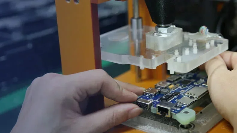
If you have spent any time in electronics manufacturing, you know this drill: the board powers up fine on the bench, passes a quick check, and ships out. Three months later, a customer reports intermittent failures on 12% of units. The root cause? A BGA solder joint with 35% voiding that degraded under thermal cycling. Nobody caught it because nobody X-rayed it.
PCBA testing is not a box to tick. It is a sequence of decisions that either catches a defect early — when rework costs pennies — or lets it ride all the way to a field return that costs hundreds or thousands.
This article walks through the PCB assembly inspections that actually matter in production, what each one catches (and what it misses), and how a sensible testing strategy looks different for prototypes versus volume runs. I will write this for both the engineer who designs the test plan and the buyer who needs to know what they are paying for.
PCBA Testing: Catch It Early or Pay for It Later
A defect found during solder paste inspection costs almost nothing to fix — wipe the board, re-print, done. That same defect found during functional test costs real rework time. Found in the field? That is a warranty claim, a recall, or a lost customer.
Here is a rough cost multiplier I have seen in production:
|
Detection stage
|
Relative cost to fix
|
|
Solder paste inspection (SPI)
|
1x
|
|
Pre-reflow AOI
|
2x
|
|
Post-reflow AOI
|
5x
|
|
ICT / functional test
|
10x–20x
|
|
Field failure
|
100x+
|
every dollar saved by skipping a test stage gets spent ten times over in rework and returns. Good PCBA manufacturers do not skip stages. They layer them.
Before the First Component: Solder Paste Inspection
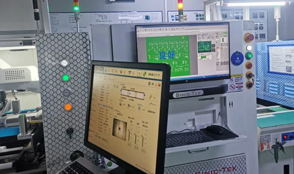
SPI happens right after stencil printing and before a single component is placed. A 3D SPI machine scans every pad on the board, measuring paste volume, height, area, and alignment against pre-set parameters.
Why 3D matters: a 2D system can tell you the paste covers the pad. It cannot tell you whether the deposit is 80µm or 120µm thick. For fine-pitch components — 0.4mm pitch QFNs, 0201 passives — that 40µm difference is the gap between a reliable joint and a tombstoned component after reflow.
At PCBONLINE, all four SMT lines run 3D SPI as standard. Every pad gets scanned. If paste volume on any pad falls outside tolerance, the board gets flagged, cleaned, and re-printed before it ever reaches the pick-and-place machine. This single step prevents roughly 60-70% of downstream soldering defects at the earliest possible point.
What SPI does not catch: component placement errors, wrong polarity, or issues that develop during reflow. That is where AOI comes in.
Dual AOI: Before and After Reflow
AOI uses high-resolution cameras and image processing to compare each board against a golden reference. The value comes from running it at two different stages.
Pre-reflow AOI catches placement issues while they are still easy to fix: a missing 0402 resistor, a reversed diode, a QFP shifted by half a pad. At this point the paste is still wet and the component can be nudged back into position with minimal effort.
Post-reflow AOI looks for what happened in the oven: solder bridges across adjacent pins, insufficient wetting on a ground pad, tombstoned chip components, lifted leads. These are harder to fix but catching them now — before the board reaches ICT or functional test — still saves hours of troubleshooting.
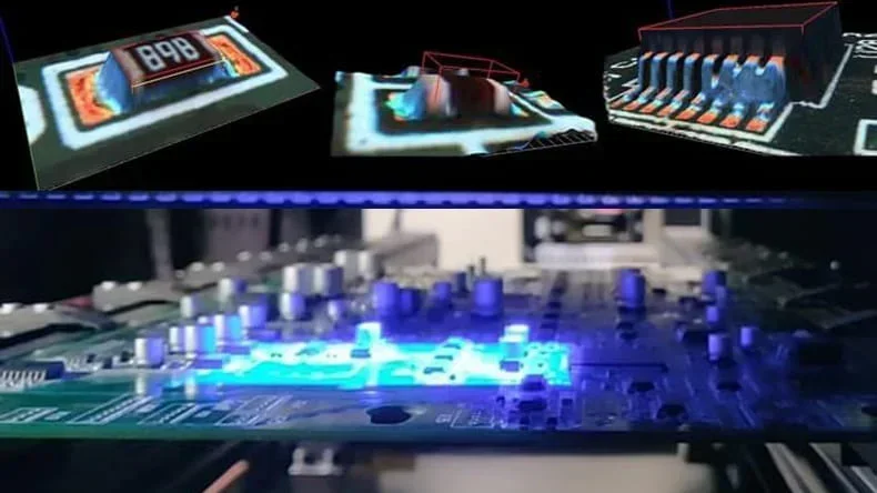
The quality of the AOI system matters more than most people realize. A 3D AOI system captures solder joint height and shape, not just 2D patterns. This means it can detect things a 2.5D system overlooks, like a slightly lifted lead that still looks fine in a top-down image.
PCBONLINE uses 3D AOI at both pre- and post-reflow positions on every SMT line. No exceptions.
X-Ray: What AOI Cannot See
AOI is surface-level. If your board has BGA packages, QFN components with exposed pads underneath, or any bottom-terminated device, the critical solder joints are invisible to optical inspection.
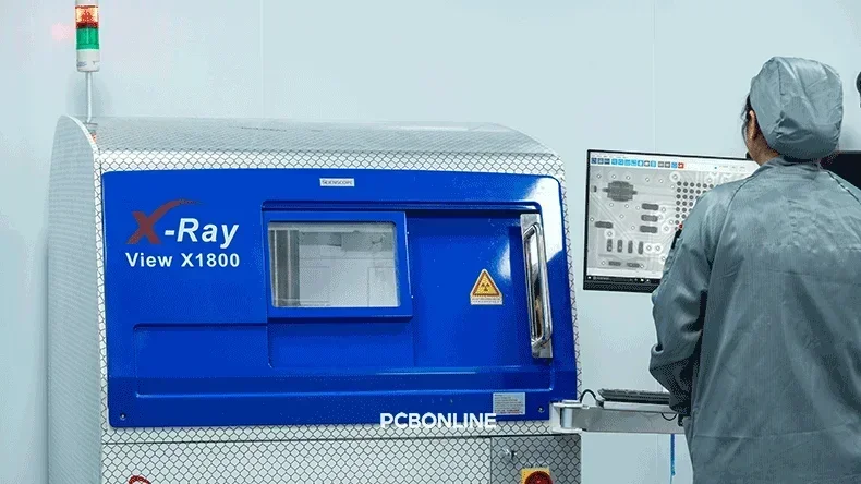
X-ray inspection penetrates the package body and reveals what is happening underneath: solder ball voiding percentage, head-in-pillow defects, bridging between adjacent balls, and cold joints where the ball never fully wetted to the pad.
For BGA components specifically, IPC-A-610 allows up to 25% voiding per individual ball. But for high-reliability applications — automotive, medical, aerospace — many customers set their own tighter limits, often 10-15%. You cannot verify this without X-ray.
PCBONLINE performs X-ray inspection on every assembly that contains BGA, QFN, or other hidden-joint components. The images and voiding analysis are included in the inspection report.
A practical note for engineers: if your design uses BGA parts, make sure your PCB layout includes at least one or two test points accessible from the bottom side near the BGA area. This gives the X-ray operator reference markers for alignment and helps correlate any X-ray findings with electrical test results later.
First Article Inspection: Check Before Volume Production
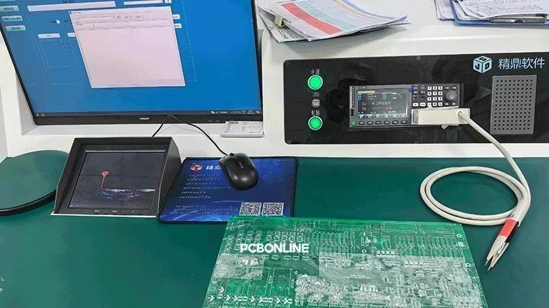
For prototype and sample orders, the most valuable single test is the first article inspection (FAI).
Here is how it works: after the first PCBA completes assembly, one board is randomly selected. A technician checks every single component on that board — verifying each resistor value, capacitor rating, diode polarity, IC orientation, and solder joint quality against the BOM and assembly drawing. The results go into an FAI report.
PCBONLINE provides FAI on all sample and prototype orders. The FAI report gets sent to the customer alongside the prototype boards for review and sign-off before any volume production begins. This gives you — the engineer or buyer — documented evidence that the assembly process is dialed in correctly.
If the FAI turns up any value out of tolerance or placement issue, it gets corrected immediately. You do not discover it three weeks later when you finally power up the boards in your own lab.
Post-Assembly Testing: ICT, Functional Test, and Burn-In
Once SMT and through-hole assembly are complete, the board moves to the post-assembly testing stage. This is where you validate that the assembled board actually works — electrically and functionally.
In-Circuit Test (ICT)
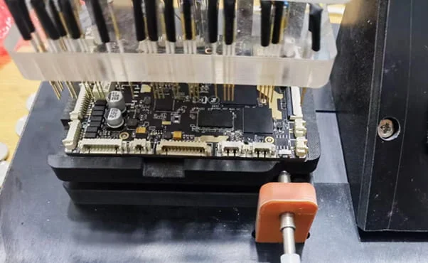
ICT uses a bed-of-nails fixture to contact test points across the board simultaneously. It verifies:
- Resistor and capacitor values within tolerance
- Diode and transistor orientation and function
- No shorts between adjacent nets
- No open circuits on critical traces
- Basic power rail voltages
ICT requires a custom test fixture, which means there is an upfront fixture design and fabrication cost. But on a per-board basis, ICT is fast — a few seconds per board — and catches the vast majority of simple manufacturing defects before you ever power the board on.
PCBONLINE designs and builds custom ICT fixtures in-house. The fixture cost is a one-time NRE; once built, it is reused across the entire production run.
Functional Test (FCT)
ICT tells you the components are assembled correctly. FCT tells you the board performs its intended function.
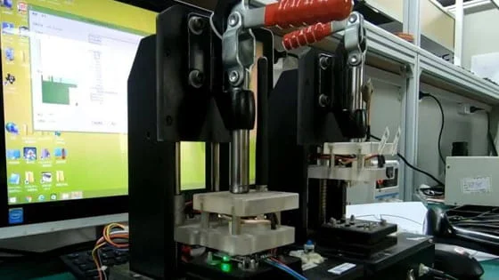
A functional test setup simulates the operating environment: applying input signals, measuring output responses, running firmware, communicating over the board's interfaces (UART, I2C, SPI, CAN, USB, Ethernet), and verifying that every subsystem behaves within specification.
Like ICT, FCT requires a custom test bench or fixture. The complexity depends entirely on the board: a simple LED driver needs a basic power-and-measure setup; an IoT gateway with multiple radios, sensors, and interfaces needs a test station that exercises every communication path and logs results with pass/fail thresholds.
PCBONLINE builds custom FCT setups for customer projects. For prototypes and small-batch orders, the FCT setup fee is often absorbed into the project cost. For volume production, the FCT bench runs as part of the standard line.
One thing worth mentioning: if your PCBA total area exceeds 3 square meters across the production order, FCT becomes especially cost-effective because the per-board cost drops significantly and the investment in the test bench pays for itself through reduced field returns.
Burn-In / Aging Test
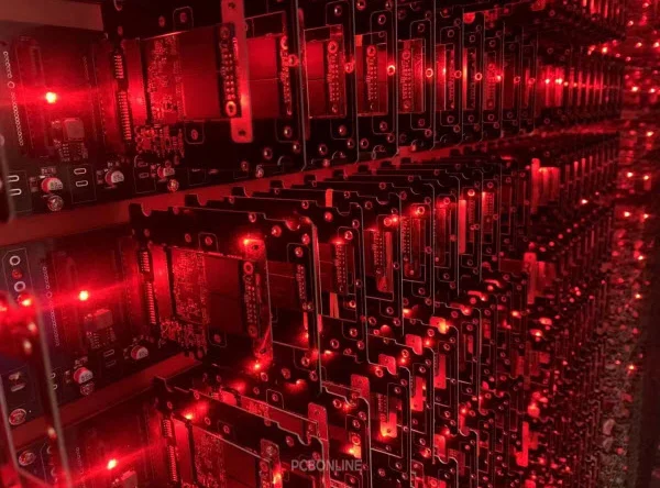
Some defects do not show up on a first-power test. They appear only after the board has been operating for hours or days — a capacitor with borderline ESR that drifts under heat, a solder joint with micro-cracking that opens after thermal expansion, an IC with latent ESD damage.
Burn-in testing runs the assembled PCBA at elevated temperature under load for an extended period — typically 8 to 72 hours depending on the product class. It screens out mortality failures before the boards leave the factory.
For high-reliability applications, burn-in is not optional. PCBONLINE offers burn-in testing as a standard post-assembly service, with temperature profiles and duration configurable to your product requirements.
Application-Specific Testing: When Standard Tests Are Not Enough
Some PCBAs face conditions that standard ICT and FCT do not simulate. These require specialized testing tailored to the product's actual operating environment.
Bending Test for Flexible PCBAs
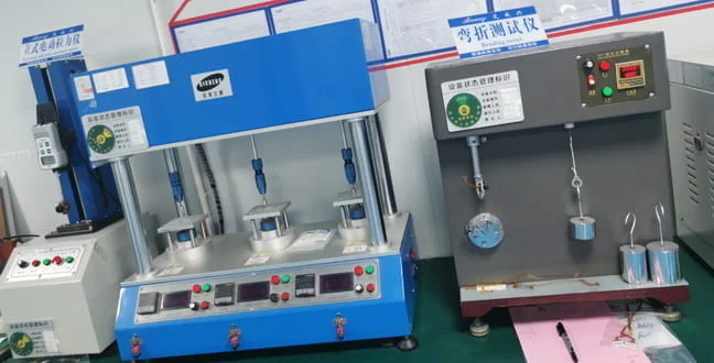
If your assembly uses a flexible PCB or a rigid-flex PCB, the board will bend in its final installation. A solder joint that looks perfect on a flat bench may crack when the board is curved around a battery or folded into a housing.
Bending tests cycle the flex PCBA through its expected bend radius — sometimes hundreds of cycles — while monitoring electrical continuity. Any intermittent opens or resistance drift gets flagged.
PCBONLINE performs bend testing for flexible and rigid-flex assemblies. The test parameters (bend radius, cycle count, angle) are set based on the product's mechanical specifications.
Salt Spray Test for Harsh Environments
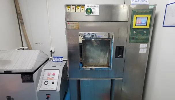
For PCBAs that will operate outdoors, in marine environments, or in industrial settings with corrosive atmospheres, salt spray testing evaluates corrosion resistance.
The test exposes the PCBA to a saline mist at controlled temperature and concentration, usually for 24 to 96 hours depending on the severity level required. After exposure, the board is inspected for corrosion on exposed copper, connector pins, and solder joints.
This is not a test you run on every board. It is a qualification test — typically done on a sample from the production batch. But if your product is going into a fishing boat or an offshore wind turbine, you want to know the results before shipping.
Button Life Test for High-Use Interfaces
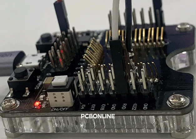
Consumer electronics, industrial control panels, and medical devices often include mechanical buttons or membrane switches that get pressed thousands of times over the product's lifespan.
A button life test uses an automated actuator to press each button repeatedly — tens of thousands of cycles — while monitoring for contact bounce, increased resistance, or mechanical failure. The test confirms that the switch assembly and its solder joints can survive the product's expected lifetime without degradation.
PCBONLINE offers button life testing for products with user-facing switches and controls. The cycle count is matched to the product's expected usage profile.
How Testing Strategy Should Change from Prototype to Volume
A common mistake: using the same test strategy for prototype builds and for mass production. They are different problems.
For prototypes, the priority is thoroughness over speed. You want every board inspected at every possible stage because the cost of discovering a design or process issue late — after you have built 50 verification units — is high. FAI, full AOI, X-ray on every board, ICT on every board. The goal is to confirm the design is manufacturable and the process is stable.
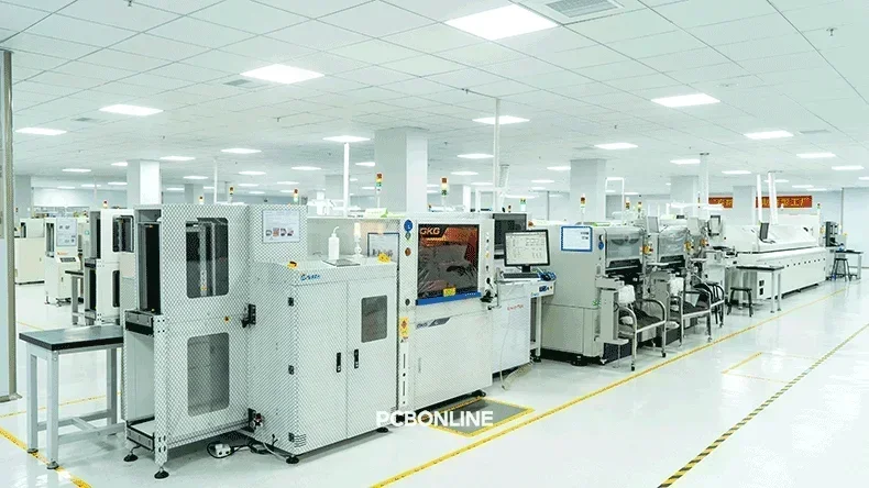
For volume production, the priority shifts to efficiency without sacrificing coverage. You build custom ICT fixtures and FCT benches that automate the testing so it runs in-line at production speed. AOI becomes a continuous monitoring tool — catching batch-level trends rather than individual one-off defects.
PCBONLINE handles both phases under one roof. The prototype runs use the same SMT lines as volume production. The test fixtures built for prototypes get reused (and refined) for volume runs. This continuity means the process you validated at prototype stage is the same process that produces your volume order — no surprises from a different factory with different equipment.
What to Ask Your PCBA Manufacturer About Testing
If you are evaluating suppliers, here are the questions worth asking — and the answers that distinguish a serious manufacturer from a box-checker:
1. Is your SPI 2D or 3D?" — 3D SPI catches thickness variation; 2D does not. For anything with fine-pitch or small passives, 2D is not enough.2. "Do you run AOI before reflow, after reflow, or both?" — "Both" is the right answer. Pre-reflow catches placement errors when they are easy to fix. Post-reflow catches soldering defects.
3. "How do you handle BGA and QFN inspection?" — The answer must include X-ray. If they say "visual inspection" or "AOI covers it," they do not understand hidden joints.
4. "Do you provide FAI reports for prototype orders?" — If they say no, ask yourself how you plan to verify the assembly before signing off on volume production.
5. "Can you build custom ICT and FCT fixtures in-house?" — Outsourcing fixture builds adds lead time and communication overhead. In-house fixture design is faster and the fixture is designed with direct knowledge of the production line.
6. "Do you offer application-specific testing like bend test, salt spray, or button life test?" — This separates a general-purpose assembler from one that works across product verticals.
PCBONLINE checks all of these boxes. Four fully automated SMT lines, 3D SPI and 3D AOI at every line, X-ray for hidden-joint components, FAI reporting on prototypes, in-house ICT and FCT fixture design and build, and application-specific reliability testing — all under one roof in Shenzhen.
FAQ about PCBA Testing
Q: What is the difference between AOI and X-ray inspection?AOI uses visible-light cameras to inspect the surface of the PCBA — component placement, solder bridges, tombstoning, missing parts. It cannot see through components. X-ray penetrates component packages and reveals hidden solder joints underneath BGAs, QFNs, and other bottom-terminated devices. AOI and X-ray are complementary, not alternatives.
Q: Do I need ICT if I already have functional testing?Yes — they catch different things. ICT verifies that every resistor, capacitor, diode, and trace is correctly assembled. FCT verifies the board performs its function. A board can pass FCT with a wrong-value pull-up resistor that causes intermittent behavior later. ICT catches that component-level error directly. For anything beyond the simplest boards, you want both.
Q: When should I run burn-in testing?Burn-in is standard for automotive, medical, aerospace, and industrial-control products. For consumer electronics, it depends on your failure tolerance — if a 2% field failure rate is unacceptable, burn-in is worth the cost. The test typically runs 8-72 hours at elevated temperature.
Q: How much does a custom ICT fixture cost?It depends on the board size, test point count, and complexity. A simple fixture for a small board with 50-100 test points might cost a few hundred dollars. A complex fixture for a large board with 500+ test points can run into the thousands. This is a one-time NRE cost that gets amortized across the production volume.
Q: Is X-ray inspection necessary for every board?If your board has no BGA, QFN, LGA, or any component where solder joints are hidden underneath the package body, then AOI alone may be sufficient. If any component has hidden joints, X-ray is essential. There is no optical workaround for seeing what is underneath a BGA.
The Bottom Line
PCBA testing is not a single step. It is a chain, and the strength of the chain is the weakest link. Skip SPI, and you let paste defects through. Skip X-ray, and BGA voids go undetected. Skip FAI, and you approve volume production without documented evidence that the prototype was built correctly.
For engineers, the takeaway is this: design your test strategy alongside your PCB layout. Include test points. Leave clearance for fixture probes. Think about inspection access before finalizing component placement.
For buyers, the takeaway is simpler: when comparing quotes, ask what testing is included — not just the headline price. A supplier that runs 3D SPI, dual-stage 3D AOI, X-ray, and full post-assembly testing will cost slightly more per board than one that runs a visual check and a power-up test. But the difference in field reliability pays for that cost difference many times over.
Turnkey PCBA Manufacturer from Prototype to Bulk Production
If you need a manufacturing partner that treats testing as a core part of the assembly process, PCBONLINE provides one-stop PCB fabrication, component sourcing, SMT assembly, through-hole assembly, and complete PCBA testing from prototype to volume production. Reach out with your Gerber, BOM, and pick-and-place file for a project review and quote.

At the turnkey OEM PCB manufacturer PCBONLINE, we not only provide PCB manufacturing and assembly from prototypes to bulk production, but also component sourcing, custom jigs and molds, conformal coating, custom enclosures, wiring cables, accessory connectors, box-build assembly, and application stimulation testing.
Founded in 2005, PCBONLINE has two large advanced PCB manufacturing bases in Jiangsu and Jiangxi Provinces in China, one turnkey PCB assembly factory in Shenzhen, and a smart OEM center and headquarter also in Shenzhen. Besides, PCBONLINE has long-term cooperation with the top 3 model manufacturers in China to provide custom jigs and enclosures for PCB assembly.
we aim to be a manufacturing partner who boosts our target customer's product success. Our target customers are terminal companies, solution companies, product companies, business makers, and research institutes. In the prototype phase, we would even pay by ourselves to complete all additional tests and certifications for your prototype quality integrity rather than just do the electronic manufacturing work.
With our OEM PCB prototype and assembly, you can ensure PCBA quality through our complete PCBA testing.

We conduct first-article inspections both before prototype assembly and before mass production to ensure the highest PCBA quality and prevent costly issues.
Each SMT line at PCBONLINE is equipped with three advanced pick-and-place machines, supporting up to 376 SMD placements per PCB, enabling us to handle all types of SMT assembly, including high-density and large-format PCBs.
PCBONLINE offers one-on-one engineering support and has expertise in hardware and software R&D from the project's early development phase to the field application engineering (FAE) stage.
By BOM component sourcing and in-stock warehousing, as well as PCB optimization advice, we reduce the circuit board assembly costs without function or quality sacrifice.
Our experienced R&D and engineering teams provide one-on-one support, solving technical and non-technical challenges while offering optimization suggestions to ensure your project runs smoothly from start to finish.
High-quality OEM PCBA manufacturing certified with ISO 9001:2015, ISO 14001:2015, IATF 16949:2016, RoHS, REACH, UL, and IPC-A-610 Class 2/3.
When your project enters the bulky production stage, PCBONLINE refunds the fees of prototyping, including its value-added services.
Whether you need PCB prototype and assembly to build consumer IoT devices, creative electronic products, auotomotive/medical-grade systems, or industrial controls, with 21 years of OEM PCBA manufacturing experience, we ensure that both electronics performance and final product presentation meet the highest standards. We look forward to your product success in the market and our long-term cooperation in bulk production. To get a quote for your PCB/box-build project from prototype to bulk production, email us at info@pcbonline.com.
PCB assembly at PCBONLINE.pdf


