

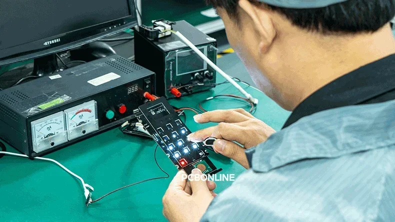
Printed circuit boards (PCB) are the foundation of all electronic products and systems. Prototyping is the first step in building electronic devices. For original equipment manufacturer (OEM) companies, solution companies, and terminal companies, PCB prototyping is vital and must provide 100% verification reliability of the product, concerning design manufacturability, testability, device functions, usage reliability, and thermal and shock durability.
There are thousands of PCB suppliers providing PCB prototypes to clients worldwide. But the thing is, how to ensure the reliability of the PCB prototypes so that the manufacturability, functions, and quality of bulk production can be foreseen, albeit with massive economic losses in the bulk production stage? Apart from that, for quality consistency, it's better to continue bulk production at the same PCB manufacturer that offers prototyping and assembly. So affordable and transparent pricing is also important.
Here are useful tips to ensure verification of the reliability of your decision in PCB prototyping and assembly. And they are simple.
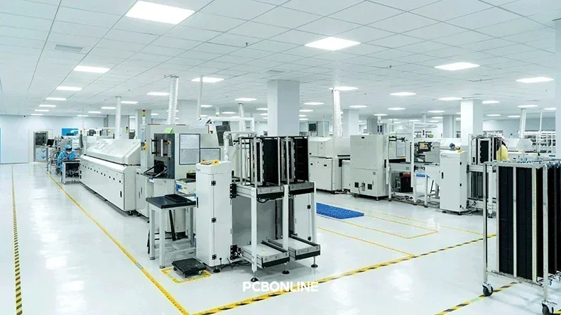
- 1. Making sure your PCB prototype is single on the production panel rather than order pooling with other designs.
- 2. Making sure your prototype PCB manufacturing and assembly processes use the same production lines as your large-scale production in the future.
- 3. Your PCB manufacturer must provide the first article inspection (FAI) after prototype assembly and offer you the FAI report.
- 4. Complete testing and inspections, including the automatic optical inspection (AOI) and flying probe/in-circuit test for PCBs, and pre- and pro-reflow AOI and functional testing for prototype PCB assembly.
- 5. It's better if your PCB manufacturer offers not only PCBs and assembly, but also custom jigs/molds, enclosures, and wiring harnesses so that the quality duty is clear rather than hands-off and duty arguments.
- 6. Your PCB manufacturer offers professional one-on-one engineering support, being your manufacturing partner rather than just prototyping without brains.
Senior engineers and project managers must understand and agree with what I am talking about. However, if you are new to the industry or if your company doesn't have enough PCB/PCBA project experience or R&D capabilities, let me explain how to ensure verification reliability of PCB prototypes and assembly in detail.
Check PCB Design Before Handing Over to the PCB House
When you complete your PCB design, you must have run the Design Rule Check (DRC), which checks the clearance, trace widths, and via sizes and ensures your design is functional. However, the DRC is not enough.
Ask yourself these questions:
Have you designed at least two pads as the test points on your PCB so that your PCB manufacturer can use the multifunctional meter to check the prototype?
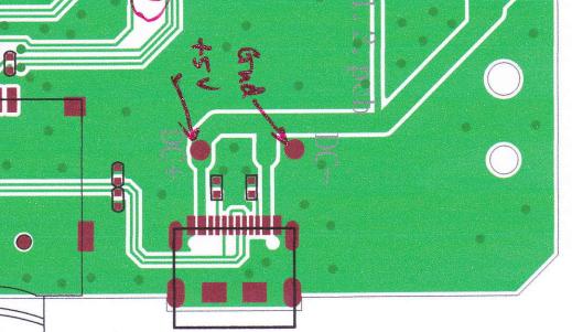
The above details won't trigger the DRC warnings, and most people won't notice them. But they do affect manufacturability, testability, and product quality. That's why you need PCB prototyping and assembly before bulk production, and it's better if your PCB manufacturer can help you debug and solve them in the design for manufacturing (DFM) and prototype phase.
Make Sure Your PCB Manufacturer Does DFM in PCB Prototype Phase
If your PCB manufacturer provides DFM for your project, that means they have engineering capabilities and experience. Speaking of professional one-on-one engineering support from the PCB manufacturer, is it important? Of course. OEM PCB manufacturers like PCBONLINE even have R&D capabilities beyond engineering support, which empowers your project success.
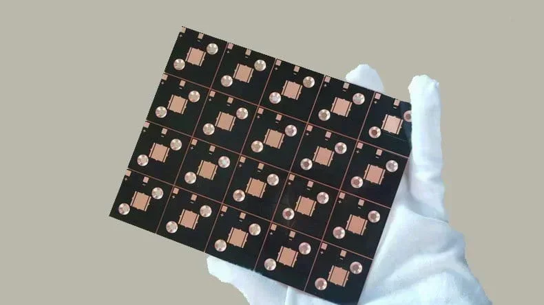
At PCBONLINE, our capabilities extend beyond PCB fabrication and assembly. Through Front-End Loading and engineering-driven DFM analysis, we help customers identify potential manufacturing risks before materials are purchased and production begins.
Let's use an example to illustrate why DFM provided by an OEM PCB manufacturer is critical.
A recent PCB assembly project for a shared scooter IoT mainboard demonstrates how early-stage DFM intervention can reduce cost, improve manufacturability, and accelerate product introduction.
Project background
A customer approached PCBONLINE with a completed IoT mainboard design. Since our team was not involved during the initial R&D phase, the design contained several hidden risks related to inspection accessibility, component compatibility, and overall production cost.
Before moving into manufacturing, PCBONLINE engineers conducted a comprehensive Production-Ready Design Review and implemented three vital improvements.
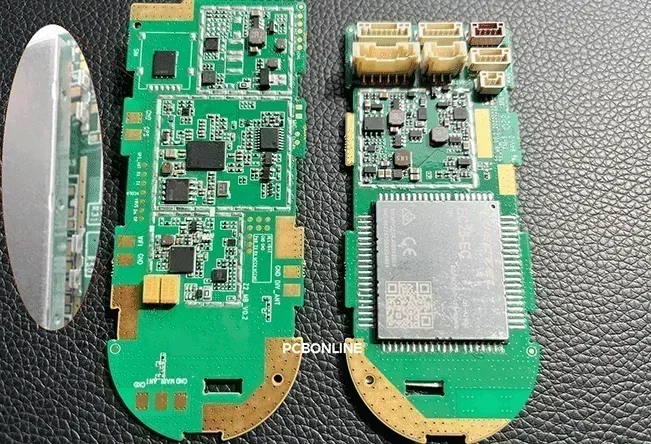
PCBONLINE's three DFM solutions are:
1. Improving inspection accessibility with shielding can optimizationChallenge
The original design used a fixed surface-mount shielding can.
After soldering, critical components underneath the shielding can, including the communication module, could no longer be fully inspected through AOI or X-ray systems. Any hidden soldering defect could remain undetected until final functional testing, increasing the risk of costly rework and delays.
SolutionPCBONLINE recommended replacing the fixed shielding structure with a snap-on shielding can.
This design change allowed SMT components to undergo complete AOI and X-ray inspection before the shielding covers were installed, improving process visibility and manufacturing yield.
ResultThe customer achieved better defect detection capability, reduced rework risk, and improved production reliability.
2. Resolving BOM and PCB footprint compatibility risks
Challenge
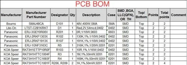
During the DFM review, PCBONLINE engineers identified mismatches between three passive component specifications listed in the BOM (Bill of Materials) and the corresponding PCB land patterns.
If discovered after production started, the inconsistencies could have caused assembly interruptions, component placement issues, and production delays.
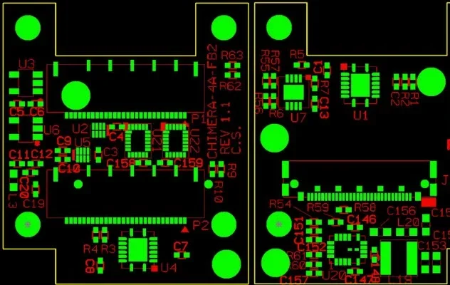
Our engineers immediately notified the customer and worked with the design team to adjust PCB pads and routing before manufacturing began.
ResultThe early correction eliminated potential assembly risks and helped ensure a smoother transition from design release to production.
3. Optimizing IoT module procurement through strategic sourcing
Challenge
IoT communication modules represent a significant portion of the BOM cost and can be affected by supply availability and market fluctuations.
Leveraging PCBONLINE's global supply-chain network and partnerships with original component manufacturers and authorized distributors, our sourcing team optimized component procurement for the project.
ResultThe customer reduced overall component procurement costs by 15%, with additional savings of approximately 10% on general passive components, while maintaining supply stability.
Only Your PCB Prototype on The Production Panel
Some PCB manufacturers, especially the 2C manufacturers that provide cheap prototypes and assembly, use order pooling to reduce production costs. It means similar PCB designs from different projects are grouped on the same production panel in prototype PCB manufacturing and assembly. Students and hobbyists will love it because it is crazily cheap!
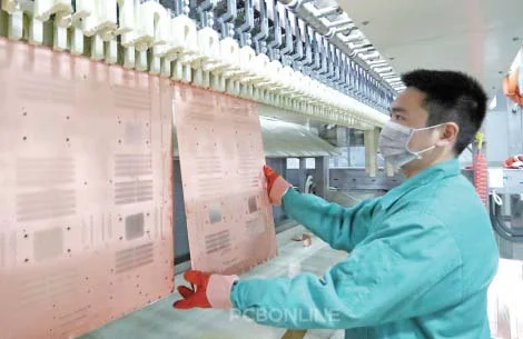
However, if you are a terminal company, solution company, product company, business maker, or research institute, NEVER attempt order pooling for your prototype!
Order pooling is cheap, but it certainly brings some quality and reliability sacrifice, especially when the prototype PCB is arranged on the edge of the production panel. Uneven via copper thickness is the problem of order pooling.
Since you are planning a formal product rather than a student thesis or a hobbyist toy, don't order pool! Spend a little more to put only your design on the production panel.
Complete Tests and Inspections
To prove the verification, the PCB prototype and assembly must undergo complete inspections and tests as bulk production will. During the PCB prototype and assembly phase, the PCB tests include at least the AOI after each time of circuit layer generation and the flying probe test after prototype PCB manufacturing, and the in-circuit test after PCB assembly.
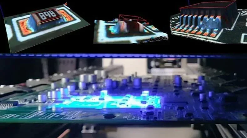
- AOI after each circuit layer generation: Both the inner layer and outer layer circuits, after pattern transfer and copper etching, require an AOI inspection to check each circuit layer to ensure the circuit pattern follows the Gerber design.
HDI PCBs, high-density flexible PCBs, and IC load boards even require AOI inspections, especially after laser drilling, via filling, solder mask application, and silkscreen printing. Additionally, X-ray inspection after each time of lamination.
- X-ray inspection: For complex integrated circuits like Ball Grid Arrays (BGAs) or Quad Flat No-leads (QFNs) where solder joints are physically hidden beneath the component package, X-ray inspection is a mandatory step. The X-ray penetrates the silicon to verify the structural integrity of every hidden electrical connection, checking for voids, cracks, or short circuits.
- First article inspection (FAI): FAI is a critical validation step included in our quick turn service. The very first fully assembled board off the production line undergoes exhaustive diagnostic checks against the original design specifications. Full production only continues once this "First Article" is verified to be 100% perfect, ensuring the manufacturing process parameters are dialed in correctly.
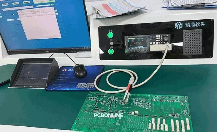
Besides, there are dual AOI inspections pre- and pro-reflow soldering to ensure component pick-and-place effect, X-ray inspection to ensure hidden-joint connection, functional testing after PCB assembly to ensure the PCBA functions, and aging testing to ensure the thermal durability and long-working-time reliability of the PCBA.
One-stop Turnkey PCB Prototype Manufacturing and Assembly
In the prototype phase, terminal companies, what the product companies, and solution companies want not the bare PCB or PCBA module, but the final device. For quality consistency, the production lines for PCB prototype and assembly are the same as bulk production. To clear the manufacturer's duty and solve issues efficiently in case of any defects in the prototype phase, it's better to work with an OEM PCB manufacturer that can complete PCB prototype and assembly until the fully inspected finished product.

At the turnkey OEM PCB manufacturer PCBONLINE, we not only provide PCB manufacturing and assembly from prototypes to bulk production, but also component sourcing, custom jigs and molds, conformal coating, custom enclosures, wiring cables, accessory connectors, box-build assembly, and application stimulation testing.
Founded in 2005, PCBONLINE has two large advanced PCB manufacturing bases in Jiangsu and Jiangxi Provinces in China, one turnkey PCB assembly factory in Shenzhen, and a smart OEM center and headquarters also in Shenzhen. Besides, PCBONLINE has long-term cooperation with the top 3 model manufacturers in China to provide custom jigs and enclosures for PCB assembly.
we aim to be a manufacturing partner who boosts our target customers' product success. Our target customers are terminal companies, solution companies, product companies, business makers, and research institutes. In the prototype phase, we would even pay ourselves to complete all additional tests and certifications for your prototype quality integrity rather than just do the electronic manufacturing work.
With our OEM PCB prototype and assembly, you can ensure the verification reliability of the prototype phase so that you can start your bulk production journey with us.
We conduct first-article inspections both before prototype assembly and before mass production to ensure the highest PCBA quality and prevent costly issues.
Each SMT line at PCBONLINE is equipped with three advanced pick-and-place machines, supporting up to 376 SMD placements per PCB, enabling us to handle all types of SMT assembly, including high-density and large-format PCBs.
PCBONLINE offers one-on-one engineering support and has expertise in hardware and software R&D from the project's early development phase to the field application engineering (FAE) stage.
By BOM component sourcing and in-stock warehousing, as well as PCB optimization advice, we reduce the circuit board assembly costs without function or quality sacrifice.
Our experienced R&D and engineering teams provide one-on-one support, solving technical and non-technical challenges while offering optimization suggestions to ensure your project runs smoothly from start to finish.
High-quality OEM PCBA manufacturing certified with ISO 9001:2015, ISO 14001:2015, IATF 16949:2016, RoHS, REACH, UL, and IPC-A-610 Class 2/3.
When your project enters the bulk production stage, PCBONLINE refunds the fees of prototyping, including its value-added services.
Whether you need PCB prototyping and assembly to build consumer IoT devices, creative electronic products, auotomotive/medical-grade systems, or industrial controls, with 21 years of OEM PCBA manufacturing experience, we ensure that both electronics performance and final product presentation meet the highest standards. We look forward to your product success in the market and our long-term cooperation in bulk production. To get a quote for your PCB/box-build project from prototype to bulk production, email us at info@pcbonline.com.
Conclusion
PCB prototype and assembly must provide 100% verification reliability. This article offers advice on how to ensure PCB prototype reliability and details it. PCBONLINE is an OEM PCB manufacturer providing turnkey electronic manufacturing from PCB prototype and assembly to box-build bulk production, and it offers one-on-one engineering support to solve technical issues. Email PCBONLINE at info@pcbonline.com and let us be your manufacturing partner.
PCB assembly at PCBONLINE.pdf


