
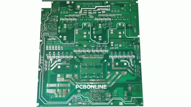
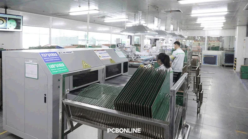
Manufacturing printed circuit boards (PCBs) is a precise, multi-stage process. It transforms a circuit design into a physical circuit board. The PCB is the backbone of modern electronic devices. At PCBONLINE, we specialize in high-quality PCB fabrication for clients around the globe. Our capabilities range from rapid prototyping to mass production.
Before putting it into PCB fabrication, we provide a free design for manufacturing (DFM), checking all your Gerber, BOM, and requirements to ensure the manufacturability of your design. If it needs any optimizations, our experienced engineers will provide suggestions to you.
The Manufacturing Printed Circuit Process
Different PCBs require different workflows and machinery for manufacturing printed circuits. For example, manufacturing high-density printed circuits (HDI PCBs) requires laser-drilling each layer and sequential lamination for creating the blind vias, while regular multilayer FR4 PCBs just need thermal lamination for one time and mechanical drilling to create the plated through holes (PTH).
Step 1: Material preparation and cutting
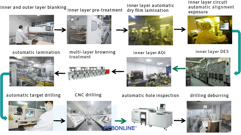
The first stage involves preparing the base material. This is typically a copper-clad laminate. This material is cut to precise dimensions. This initial sizing aligns with design specifications. Automated blanking machines ensure accuracy. Edging and filleting remove burrs. This prevents quality issues. PCBONLINE utilizes various laminate materials. Copper thickness can vary (e.g., H/Hoz, 1/1oz, 2/2oz). This depends on specific PCB requirements.
Step 2: Inner layer circuitry creation
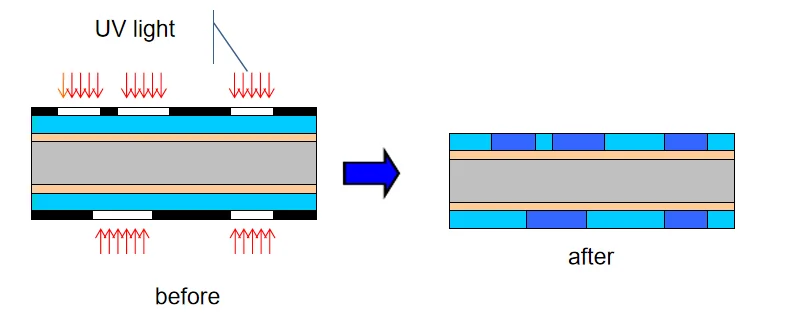
Inner-layer circuits are essential. They form the internal electrical pathways. This step uses an image transfer method. First, the laminate undergoes pretreatment. This cleans the surface. It also enhances roughness for better adhesion. A photosensitive dry film is then applied. This film is sensitive to UV light. Circuit patterns are precisely aligned. They are exposed to UV light. This transfers the design onto the film.
Next, the exposed panels enter the Develop, Etch, and Strip (DES) line. The unpolymerized film is removed during development. Unwanted copper is then etched away. This leaves the circuit traces. The remaining resist is stripped off. Automated Optical Inspection (AOI) follows this. AOI is crucial for detecting defects. It ensures the integrity of the inner-layer circuits. PCBONLINE's advanced processes guarantee flawless inner layer patterns. This is vital for complex designs, including HDI PCBs.
Step 3: Multi-layer lamination
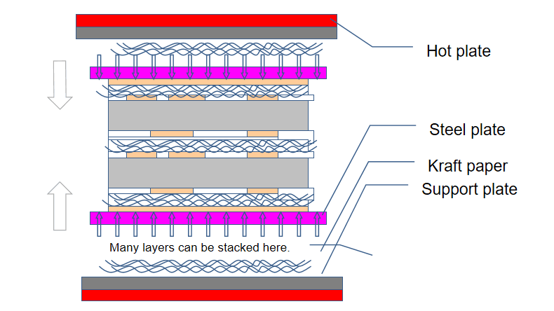
Multi-layers in a PCB are bonded together. The lamination process involves stacking inner layers. Pre-preg (pre-impregnated material) and copper foil are added. These layers are then pressed under high heat and pressure. This creates a solid, unified board. For HDI PCBs, lamination can be sequential. This involves multiple pressing cycles. A browning treatment line ensures strong adhesion. This process is critical for building HDI PCBs. It achieves high-density interconnects. PCBONLINE's controlled lamination processes ensure perfect alignment and bonding for up to 8 lamination cycles, accommodating complex HDI builds like 1+N+1, 2+N+2, and even 4+N+4.
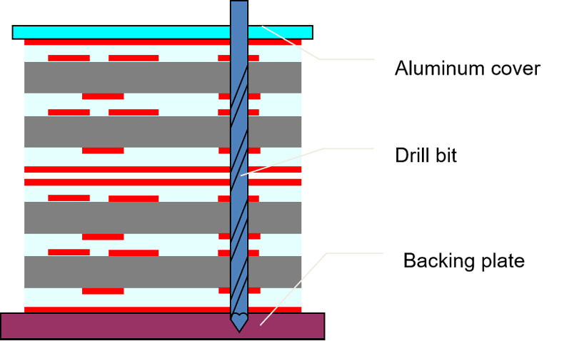
Step 4: Precision drilling
Drilling creates holes. These holes are essential for interconnections. They also serve for component mounting. PCBONLINE uses high-precision CNC (Computer Numerical Control) and automatic target drilling machines. This ensures accuracy. After drilling, deburring removes rough edges. This prepares holes for plating. An inspection machine checks hole quality. For HDI PCBs, microvias are common. These are very small holes. They are drilled using CO2 or UV lasers. Laser drilling allows for smaller vias. This enables higher circuit density.
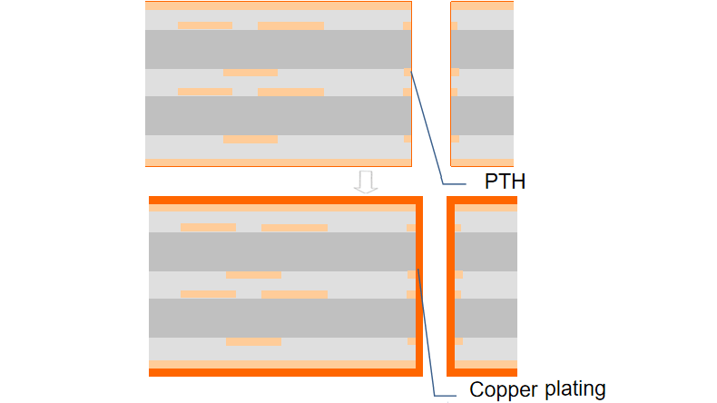
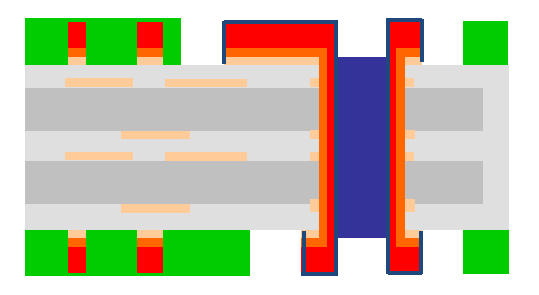
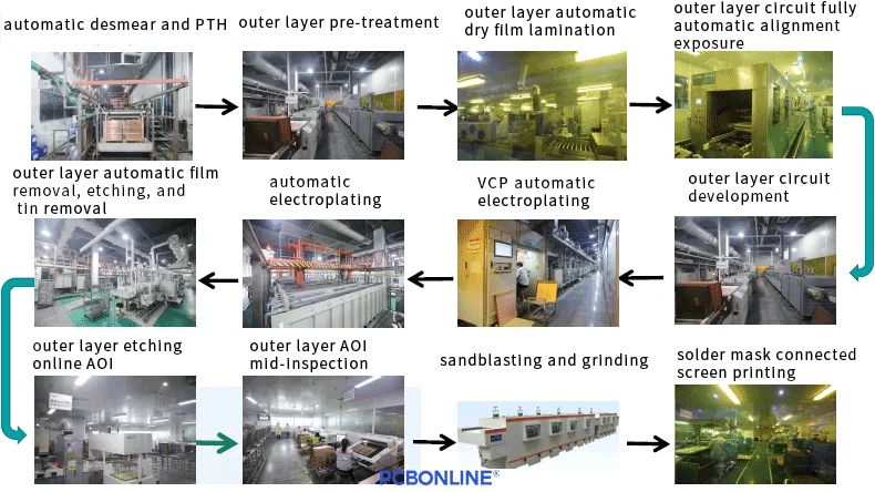
Step 5: Desmear and plating through hole (PTH)
After drilling, panels undergo desmear. This process removes resin residue. It prepares the PTH hole walls. Then, Plating Through Hole (PTH) begins. Copper is chemically deposited into the holes. This creates conductive paths. These paths connect different layers of the PCB. This electroless copper deposition forms a uniform layer. PCBONLINE uses Vertical Continuous Plating (VCP) lines. These lines ensure even copper deposition. This applies to both traces and PTH holes.
Step 6: Outer layer circuitry definition
Outer layers are also critical. They contain the external circuit patterns. This process is similar to inner layer imaging. Outer layers are pre-treated. A dry film is applied. A precise alignment exposure system transfers circuit patterns. The outer layers are then developed. Etching removes excess copper. This reveals the final circuit traces. Tin is then stripped off. This finalizes the outer layer patterns. PCBONLINE employs online AOI. This system inspects the outer layer etching in real-time. It identifies any defects. This ensures high quality and precision.
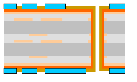
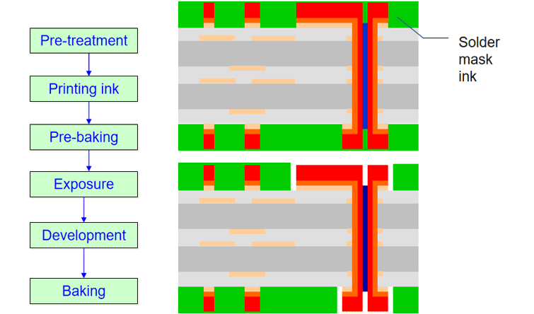
Step 7: Pattern plating and solder mask application
Pattern plating increases copper thickness. This applies to traces and pads. It strengthens the conductive pathways. After plating, the solder mask is applied. This is a protective layer. It covers non-solderable areas. It insulates traces. It also protects against environmental conditions. Solder mask is typically a liquid photoimageable (LPI) ink. It is applied over the entire board. UV light then exposes specific areas. This hardens the mask. Unexposed areas are removed. PCBONLINE ensures precise solder mask application. This provides maximum protection for your circuits.
Step 8: Legend (silkscreen) printing
The legend, or silkscreen, adds essential markings. These include component designators. They also show polarity indicators and logos. These markings aid in assembly and troubleshooting. A non-conductive epoxy ink is used. It is typically white or yellow. This ink is screened onto the board surface. The board then passes through a curing oven. This permanently bonds the ink. PCBONLINE's precise silkscreening ensures clear and durable markings.
Step 9: Surface finish application
Surface finish protects exposed copper. It prevents oxidation. It also ensures solderability. Various surface finishes are available. Common options include ENIG (Electroless Nickel Immersion Gold), HASL (Hot Air Solder Leveling), Immersion Tin, and OSP (Organic Solderability Preservative). Each finish has unique properties. They suit different application requirements. PCBONLINE offers a range of surface finishes. We help clients select the best option for their specific needs.
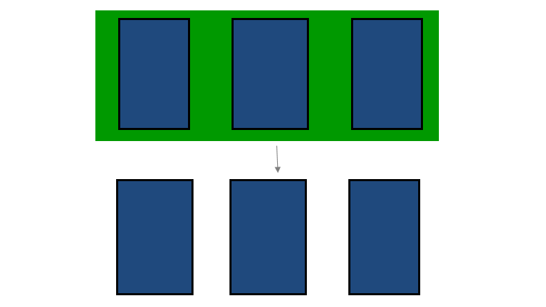
Step 10: Profiling (routing and V-cut)
Profiling is the final cutting stage. It shapes the PCB to its required dimensions. This includes routing and V-cutting. Routing uses a CNC machine. It precisely cuts the board outline. V-cutting creates V-shaped grooves. This allows for easy separation of multiple boards from a panel. PCBONLINE's advanced profiling equipment ensures precise board dimensions.
Step 11: Electrical testing
Every PCB undergoes rigorous electrical testing. This identifies any manufacturing defects. It separates non-functional boards. This prevents economic losses in downstream processes. During PCB fabrication, the flying probe test is conducted to ensure electrical connections.
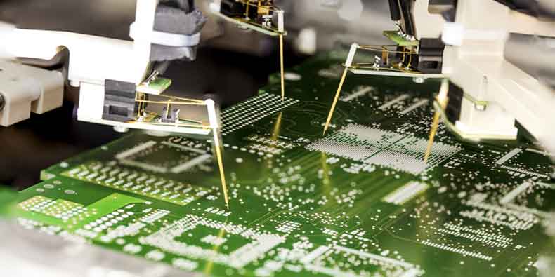
Flying probe testing: This uses robotic probes. They move across the board. They make contact with test points. This method is flexible. It is suitable for prototypes and low-volume production.
PCBONLINE conducts comprehensive electrical tests. This guarantees the functionality of every board.
Step 12: Final quality control (FQC)
Final Quality Control is the last stage. PCBONLINE's FQC process ensures all boards meet strict quality standards. This commitment to quality is why PCBONLINE is a trusted partner.
- Dimension inspection: Outline, hole to edge, PCB thickness, hole diameter, line width/space, annular ring, bow and twist, plating thicknesses.
- Surface inspection: Checks for voids and other surface defects.
Advanced HDI Printed Circuit Manufacturing
Manufacturing high-density printed circuits is more complex, as HDI PCBs feature microvias, fine traces, and high circuit density. PCBONLINE is a leader in HDI PCB manufacturing. Compared with the above process, our HDI PCB manufacturing process for HDI PCBs is distinct for the following extra steps:
- Laser drilling: Microvias are drilled with lasers on single copper layers prior to lamination.
- Microvias enable high-density routing. PCBONLINE's minimum laser drill diameter is 0.075mm.
- Serial lamination cycles: HDI PCBs require sequential lamination. Layers are precisely aligned and bonded multiple times. This builds up the desired structure. PCBONLINE can handle up to 8 lamination cycles.
- Desmear for microvias: Ensure conductive pathways in microvias.
- VCP automatic electroplating: Ensures uniform copper deposition. This is critical for fine-pitch HDI designs.
- Online AOI and mid-inspection: Real-time inspection at various stages. This detects defects early in the HDI process. PCBONLINE has both online AOI and mid-inspection for outer layer etching.
PCBONLINE offers diverse HDI builds. These range from 1+N+1 to 4+N+4. Our expertise ensures optimal performance for high-speed circuits. This includes applications in telecommunications and advanced computing.
Machinery for Manufacturing Printed Circuit at PCBONLINE
Our two large manufacturing bases, in Jiangxi and Jiangsu Provinces, are equipped with advanced machinery for independently manufacturing printed circuits.
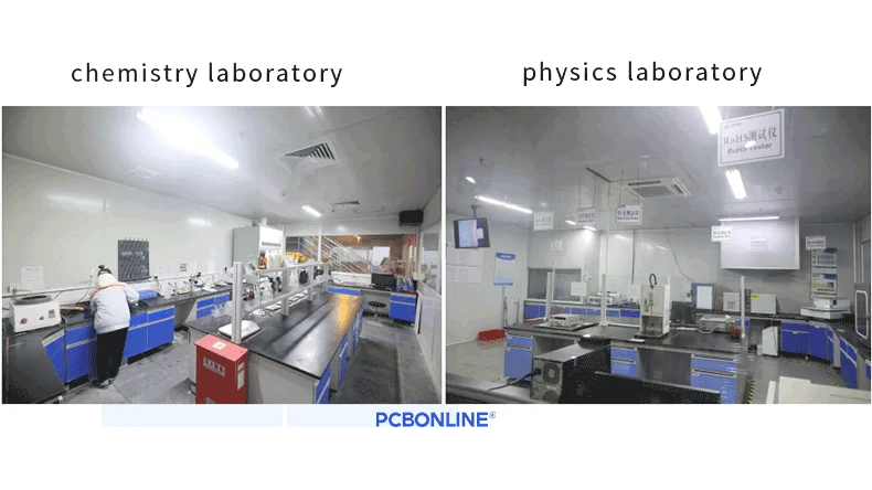
Chemical and physical laboratories
Our PCB factory in Jiangsu houses two chemical and physical laboratories, which ensure material quality and process control.
Chemistry laboratory:
- ICP-OES (inductively coupled plasma optical emission spectrometry): Analyzes metal ion concentrations. This includes copper, nickel, and iron. It is used in plating and etching solutions. Also for wastewater.
- UV-Vis spectrophotometer: Measures organic compounds. This includes developers and stripping agents. It monitors solution concentrations.
- ICP-MS/OES: Ensures compliance with environmental regulations. Specifically for RoHS/EPA wastewater discharge.
- Mercury analyzer: Detects mercury ions in wastewater.
- pH/ORP/conductivity meters: Monitors wastewater treatment processes.
- TOC analyzer (total organic carbon): Measures organic pollution in wastewater.
- Acetone wipe test: Qualitatively checks resin curing.
- Fume hoods: Handles corrosive acids and solvents safely.
- Explosion-proof refrigerator: Stores flammable chemicals.
- Waste liquid collection system: Segregates spent acids and heavy metal waste.
Physics Laboratory
- High-voltage insulation tester: Checks electrical insulation properties of PCBs.
- Resistance tester: Measures the electrical resistance of circuits.
- Peel force tester: Evaluates adhesion strength of copper traces.
- Impedance tester: Measures characteristic impedance of transmission lines. This is crucial for high-speed designs.
- RoHS tester: Ensures compliance with hazardous substance restrictions.
- Soldering ovens: Used for thermal reliability testing.
- AAS atomic absorption spectrophotometer: Analyzes the elemental composition of materials.
- Plating layer thickness tester: Measures the thickness of plated layers.
Manufacturing and Testing Equipment
PCBONLINE's factories feature a wide array of advanced manufacturing equipment.
- High-precision drilling machines: Mechanically drill holes. Essential for component placement and interconnections.
- Lamination machine: Presses layers together under high temperature and pressure. Forms a solid, unified board.
- VCP plating line: Vertical Continuous Plating lines. Ensures uniform and high-quality copper deposition.
- Automatic optical inspection (AOI) machines: Perform automated visual inspection. Detects defects in inner and outer layers. Also for solder paste and post-reflow.
- X-ray inspection machines: Used for inspecting connections under BGAs. This happens before reflow soldering.
- Flying probe testers: For electrical testing of bare boards.
- CNC routing machines: Precisely cut the PCB outline.
- Laser drilling machines: For creating microvias in HDI PCBs.
With the comprehensive manufacturing and testing equipment at PCBONLINE, we have the capabilities to seamlessly manufacture printed circuits. From design to delivery, we ensure excellence.
Why Choose PCBONLINE for Manufacturing Printed Circuit Boards
With 20 years of printed circuit manufacturing expertise, advanced equipment and facilities, and strict quality control, PCBONLINE stands out as a reliable advanced PCB manufacturer for mid and high-end applications.
Founded in 2005, PCBONLINE has two advanced PCB manufacturing bases in Jiangsu and Jiangxi Provinces, one turnkey PCB assembly factory in Shenzhen for PCBA and box builds, and an R&D team.
We offer a one-stop solution, including DFM, PCB fabrication, PCB assembly, and box-build assembly, from prototyping to mass production.
The professionals at PCBONLINE provide one-on-one engineering support and can optimize your design to reduce fabrication cost without function and quality sacrifice.
We can manufacture printed circuits for all types of boards, including HDI, rigid-flex, metal-core, ceramic, and high-frequency boards.
PCBONLINE manufactures, assembles, and tests PCBs and PCBAs to box builds as a source factory manufacturer under one roof, saving costs and time for you.
High-quality PCBA manufacturing certified with ISO 9001:2015, ISO 14001:2015, IATF 16949:2016, RoHS, REACH, UL, and IPC-A-610 Class 2/3.
PCBONLINE can reduce component costs for our clients. We source components by integrating all BOMs of our clients to lower the unit prices, and we find the original components at the lowest costs from our global supply network due to regional price differences.
When your PCB project enters mass production, we refund the fees for prototypes and offer free PCBA functional testing.
Whether you need FR4 multilayer PCBs, HDI PCBs, flexible PCBs, etc, we have the equipment, experience, and capabilities to manufacture printed circuits meeting your project requirements. To get a quote for printed circuit manufacturing, email us at info@pcbonline.com.
Conclusion
This article reveals the manufacturing printed circuit process and machinery at PCBONLINE. Partner with PCBONLINE for reliable, high-performance printed circuit boards.
PCB assembly at PCBONLINE.pdf


