
An inverter printed circuit board (PCB) is a high-power control board whose core function is to convert direct current (DC) into alternating current (AC). Inverter PCBs are essential in solar inverters, electric vehicles, industrial motor drives, uninterruptible power supply systems, and energy storage equipment.
PCBONLINE provides turnkey PCB assembly for inverters used for automotive, solar energy storage, industrial UPS systems, motor drives, etc. Our engineering team ensures all our inverter PCBs reliably handle high voltage, large current, and severe thermal stress.

How Does An Inverter Printed Circuit Board Work
An inverter printed circuit board serves as the high-speed switching hub of a power electronics system. At its center is a power stage arranged in a Full-Bridge or Three-Phase Bridge topology, which is comprised of high-performance semiconductor switches, such as MOSFETs, IGBTs, or Silicon Carbide (SiC) devices.
The inverter PCB controls power semiconductor components, such as MOSFETs, IGBTs, or SiC devices, to rapidly switch DC power. This is how:
The PCB's controller, MCU or DSP, executes high-frequency Pulse Width Modulation (PWM). The semiconductor switches are toggled on and off at frequencies ranging from 20 kHz to over 100 kHz. By precisely varying the duty cycle of these pulses, the PCB synthesizes a waveform that mimics the area under a sine wave.
The raw output from the switching semiconductors is a high-frequency square wave (PWM train). To achieve a stable AC output, the PCB utilizes an LC Filter, which is an inductor and a capacitor. The inductor resists rapid changes in current, smoothing the pulse train, and the capacitor shunts high-frequency noise to ground. Together, they integrate the pulses into a clean, low-distortion Pure Sine Wave, suitable for sensitive electronics or grid injection.
Through this switching and filtering process, DC input from sources like solar panels, battery packs, or rectified grid power is converted into a stable AC output with controlled voltage and frequency.

Features of An Inverter Printed Circuit Board
Thick copper, a large PTH area, high power density, high voltage, and harsh operating conditions are the features of an inverter printed circuit board.
Thick copper
To carry large currents safely, inverter PCBs use thick-copper construction. The copper thickness commonly ranges from 3 oz to 10 oz, and can be higher in extreme cases.
Thick copper reduces voltage drop, heat generation, and power loss. Also, it improves mechanical strength for heavy components.
At PCBONLINE, we can produce thick-copper PCBs from 3oz to 14oz.
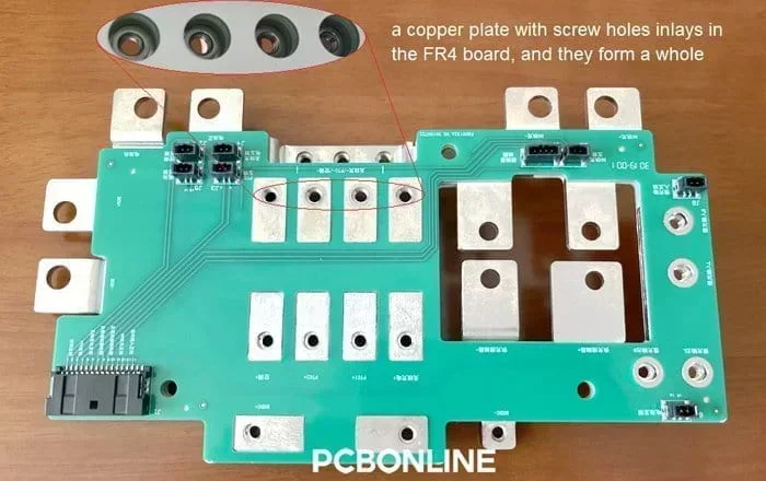
A large area of PTH assembly
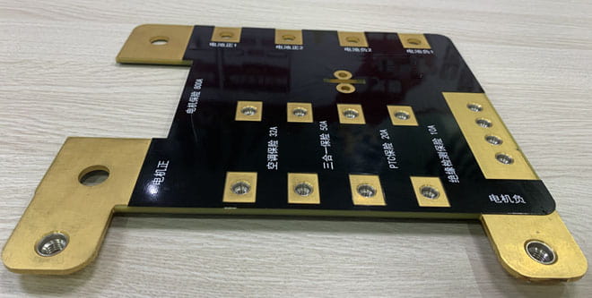
An inverter PCB relies heavily on through-hole technology (THT) for large components like capacitors and connectors.on an inverter PCB, there's a large PTH area for soldering power devices, bus connections, DC link capacitors, inductors, and terminals.
Inverter PCBs require 100% solder vertical fill (PTH hole fill) and solder volume. This requires a powerful manufacturing capability from the PCB manufacturer. PCBONLINE has rich experience in wave soldering oven temperature control and fixture design to ensure no PTH component displacement. We use laser soldering for the connection of PCB busbars and the inverter PCB. And we can use selective soldering for the PTH assembly when needed.

Strong & weak current segregation
Inverter PCBs always separate power circuits for the DC bus, phase output, and switching nodes, and control and sensing circuits for the MCU, gate drivers, and feedback.
For the strong and weak current segregation, there's usually physical zoning of the PCB, with independent ground returns and isolation components. Also, we use busbars for high currents' path, and PCB traces for weak currents' path.
For example, in the below inverter PCB manufactured by PCBONLINE for electric vehicles' changing pile, where we engaged the PCB design, we separated the networks of strong and weak currents. We use the busbars for high currents and thermal dissipation, and 3oz PCB traces for weak currents and signal transfer.
Strict creepage and clearance control
Inverter PCBs simultaneously handle high current paths and high voltage nodes. High-current and high-voltage operation demands large creepage distances on the PCB surface, adequate clearance through air, and slots, cutouts, or isolation barriers.
Routing out sections of the PCB in the design prevents arcing or flashover between high-voltage and low-voltage sections, especially in humid or contaminated environments.
High thermal load and heat dissipation design
Inverter PCBs generate significant heat due to switching losses and conduction losses. Thermal performance is as critical as electrical performance. Thermal features of an inverter PCB include:
- Thick copper acting as a heat spreader
- Large copper areas under power devices
- Thermal vias connecting to the inner or backside copper
- Direct mounting to heat sinks or cold plates
Low parasitic inductance and high EMC requirements
On an inverter PCB, there are fast switching devices, such as IGBT, SiC, and MOSFET. The PCB requires short, wide current loops, minimized loop area for DC bus and phase paths, and close placement of DC link capacitors to power devices.
Besides, inverters are strong noise sources due to high-frequency switching. To meet the EMC requirement, the PCB design should include snubber circuits, shielded gate drive routing, controlled impedance paths, and segmented ground planes.
Inverter PCB Design Requirements
In automotive and industrial environments, inverter PCBs must withstand vibration, shock, and thermal cycling. The PCB design requires thicker copper, stronger pad designs, and firm anchoring of heavy components.
Because of thick copper and large pads, the solder mask design is tightly controlled. Large current pads often require full or partial solder mask opening. The exposed copper allows additional solder buildup to reduce contact resistance, and mask openings must be well defined to avoid solder bridging and uneven wetting. When dealing with solder mask opening and tinning on the large-current path, ensure a sufficient solder mask bridge of at least 0.2mm from the solder mask opening edge to the adjacent trace.
When dealing with clearance and creepage distance, increasing pad and trace spacing, add slots or cutouts of 1.0mm+ in the PCB, and apply conformal coating when required. For 400V to 800V inverter PCBs, the minimum clearance is 3.0mm, and the minimum creepage distance is 5.0mm. This is the industrial-class standard. For 800V inverter PCBs, the minimum clearance is 4.5mm-5.5mm, and the minimum creepage distance is 8.0mm. This is the automotive-class standard.
To support heavy copper and large components, the inverter PCB thickness is usually increased to 2.0mm, 2.4mm, or 3.2mm to prevent warping or cracking under thermal stress.
Inverter Printed Circuit Board Assembly
Due to the heavy copper and the PCB busbars, inverter PCB assembly requires higher reflow and wave soldering temperatures. While typical reflow profiles peak at around 245°C, inverter PCBs require 260°C - 265°C or longer soaking times to ensure the high thermal mass components reach the wetting temperature.
Besides, inverter PCBs rely on through-hole assembly for large components like capacitors and heat sinks. The PTH assembly of inverter PCBs requires 100% solder vertical fillet and solder volume.
We pay attention to wave soldering fixture design, reflow and wave soldering oven temperature control, and manufacturing process design. We can also offer selective soldering to replace wave soldering for preventing soldering defects and component displacement if needed.
Regarding the quality control of inverter PCB assembly, we have four-terminal sensing during PCB fabrication to eliminate lead resistance for precise low-resistance measurement. We also have copper thickness inspection. During inverter PCB assembly, we have dual automated optical inspections (AOI) and X-ray inspection to ensure that the solder joints inside the thick-copper through-holes meet Class 3 standards.
Partner with PCBONLINE for Inverter Printed Circuit Boards
PCBONLINE is an OEM industrial control and automotive PCB assembly manufacturer providing free DFM (design for manufacturing) and one-stop PCBA manufacturing. You can work with PCBONLINE to turn your design into real inverter PCBs from prototypes to mass production.
Founded in 2005, PCBONLINE has two large advanced PCB manufacturing bases, one PCB assembly factory, an R&D team, and stable supply chains for components and materials.
PCBONLINE has dominant advantages in industrial control and automotive inverter PCBs. We can deal with power management, jig design, temperature control, PCB optimization, and resistance control excellently.
We have comprehensive production lines and equipment for inverter PCB assembly, from PCB manufacturing and assembly, to tests and value-added, including four-terminal sensing, copper thickness inspection, etc.
PCBONLINE offers free DFM before and during PCBA prototyping to debug design defects and solve unexpected issues to ensure the success of your inverter PCB, including Gerber, BOM, manufacturing process design, testing, burn-in, IC programming, and enclosure.
We have advantages in high-power PCB manufacturing and assembly, including thick-copper PCBs 3oz to 14oz, copper busbars, and wave soldering for large THT components without displacement.
Our one-stop inverter PCB PCB assembly capabilities include independent advanced manufacturing, 4 automatic SMT lines, 4 THT assembly, 2 X-ray inspection machines, 1 first article inspection system, conformal coating machines, burn-in cabinets, IC programmers, a component warehouse, stable supply chains, an R&D team, etc.
When your inverter PCB assembly project goes to mass production, PCBONLINE will refund you the fees of R&D, prototyping/sampling, and offer free PCBA functional testing.
High-quality inverter PCB assembly and final product assembly certified with IPC-A-610 Class 3, ISO 9001:2015, IATF 16949:2016, RoHS, REACH, and UL.
PCBONLINE has manufactured many successful inverter PCBs for industrial control and automotive applications. To get a quote for your project's inverter PCB assembly, please email info@pcbonline.com. Once you contact us, we will provide you with one-on-one engineering support.
Conclusion
Inverter PCBs are high-power and thick-copper PCBs through-hole mounted with large capacitors, heatsinks, and inductors, and surface-mounted with an MCU and driver IC. Inverter PCBs require copper thickness test, four-terminal sensing, and IPC-A-610 Class 3 acceptance standards. To ensure the success of your inverter PCB project for industrial control, automotive, motor drives, solar energy storage equipment, etc, get one-stop PCBA manufacturing services from the inverter PCB assembly manufacturer PCBONLINE.


