
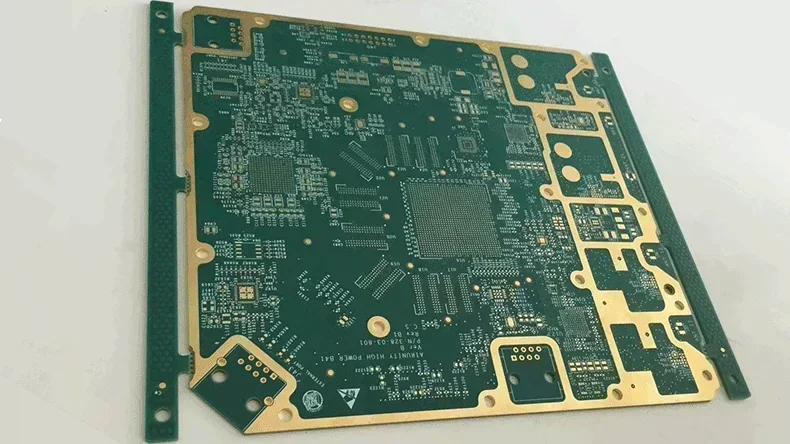
HDI PCB for AI servers made by PCBONLINE
As the demand for artificial intelligence (AI) hardware, such as AI computing power and high-speed network equipment, is growing rapidly, high-density-interconnect printed circuit boards (PCBs) used for these applications are also experiencing a booming market. PCBONLINE, a one-stop HDI PCB manufacturer, provides high-density-interconnect PCB manufacturing and assembly for BGA, high-speed network equipment, GPU AI servers, and AI computing. In this article, we will explore what high-density interconnect means, what an HDI PCB is, and introduce the high-density interconnect PCB applications in AI hardware.
What is High-Density Interconnect
High-density interconnect, abbreviated as HDI, commonly means HDI PCB in engineering. However, not only PCBs use the HDI technology, IC package substrate boards and system-in-package (SiP) / multi-chip module (MCM) also use it.
So what is the high-density interconnect technology?
HDI is a design and manufacturing technology that achieves higher interconnection density and smaller feature sizes within limited space.
It's important to note that HDI is defined by interconnection density and fabrication features, not merely by the number of layers. The key idea of high-density interconnect is to realize:
- denser routing,
- smaller pads and vias,
- thinner dielectric layers,
- higher interlayer connectivity efficiency.
HDI came from PCB technology, but today it generally refers to any high-density interconnection structure. Besides PCB technology, IC package substrates and SiP/MCM also use the HDI technology. You can learn them from the following table.
|
Application field
|
HDI used?
|
Description
|
|
HDI PCB
|
Yes, the most common HDI application
|
Uses microvias (laser vias), blind/buried vias, thin dielectric layers
|
|
IC package substrate
|
Yes, a more advanced HDI form
|
Finer line/space (<15μm), smaller vias
|
|
System-in-package (SiP) / Multi-chip module (MCM)
|
Yes
|
High-density interconnect between chips; substrate behaves like an HDI PCB
|
|
On-chip interconnect (semiconductor level)
|
No
|
But still represents a "high-density interconnect" at the silicon level
|
High-Density Interconnect PCB and Fine-Pitch Assembly
The assembly of HDI PCBs requires fine-pitch PCB assembly, but fine-pitch assembly can also be applied to other PCBs. To understand their relationship, let's first explore HDI PCBs and fine-pitch assembly.
What is HDI PCB?
A HDI PCB is a circuit board using blind/buried/micro vias and design techniques that increase interconnection density. It is characterized by: microvias, blind/buried vias, fine line/space, and dense interconnection structures, not simply by having more than four layers.
|
Feature
|
Description
|
|
Blind via
|
Connects the outer layer to the inner layer without going through the entire PCB
|
|
Buried via
|
Connects inner layers only, invisible from the outside
|
|
Microvia
|
Via diameter ≤ 150 μm, laser-drilled
|
|
Fine line/space
|
Line width and spacing ≤ 75 μm
|
|
Layer stackup
|
X+N+X (X: integer from 1 to 6), or any-layer interconnect structures
|
|
High routing density
|
A much higher number of traces or vias per unit area compared to normal PCBs
|
HDI PCBs are used more and more for electronic devices with compact sizes, such as smartphones, laptops, high-speed equipment, RF systems, network equipment, AI hardware, etc. HDI PCBs provide these advantages:
- Achieve higher signal density in a limited space
- Improve signal speed and integrity
- Reduce parasitic effects
- Save size and weight
What is fine-pitch assembly?
If the center-to-center distance between two adjacent pads or solder balls is ≤ 0.65mm, we call it a fine-pitch. A PCB with BGA, CSP, or 0402/0201/01005 components require fine-pitch assembly. Fine-pitch assembly is necessary for HDI PCBs to achieve proper fan-out and signal routing.
From the following table, you can learn what pitches different components require for PCB assembly.
|
Components
|
Ball/pad pitch
|
PCB structure
|
|
BGA
|
0.65 mm
|
HDI 1 + N + 1 (single-step microvia)
|
|
BGA
|
0.4 mm
|
HDI 2 + N + 2 or any-layer interconnect
|
|
CSP/WLCSP
|
≤ 0.3 mm
|
Any-layer HDI
|
|
0402 / 0201 / 01005
|
0.5mm/0.3mm/0.2mm
|
Requires ultra-fine line/space and precision (±15μm) SMT placement
|
Besides HDI PCBs, fine-pitch assembly and components can also be used on standard multilayer PCBs in lower-density systems.
Why do HDI and fine-pitch often coexist?
High-density-interconnect and fine-pitch often appear together because of routing constraints, miniaturization trend, and signal integrity requirements.
Routing constraints
For BGAs with ≤ 0.65 mm pitch, traditional through-holes cannot fan-out traces between pads.
Blind or laser-drilled microvias (often via-in-pad) are required to route signals from outer to inner layers.
Miniaturization trend
As packages evolve from QFP, BGA, and CSP to WLCSP and PoP, the interconnect pitch decreases. Correspondingly, PCB technology progresses from standard multilayer to HDI to any-layer interconnect.
Signal integrity and high-speed requirements
- High-speed differential pairs (DDR, PCIe, USB 3.x, SerDes, etc.) demand short paths and controlled impedance.
- HDI structures with microvias and thin dielectrics minimize stubs and parasitic effects.
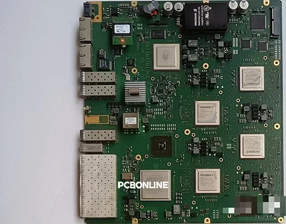
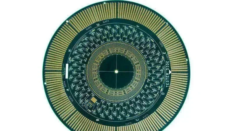
High-Density Interconnect PCB Applications in AI Hardware
HDI PCBs are widely used in AI hardware, especially high-density GPU PCBs with 24+ layers. They are used for high-performance computing and high-speed signal transmission.
In AI electronics fields, high-density interconnect PCBs are used in high-performance computing, high-speed networking & communication equipment, high-density storage & memory, and AI edge devices & high-speed industrial control.
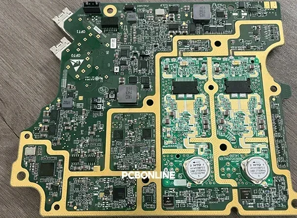
1. High-Performance Computing
24+ layers HDI feature ultra-high signal integrity, differential pairs, stacked microvias, and strict power/ground plane design. They are used in:
- AI training and inference servers,
- high-performance workstations
- Xilinx / Intel FPGA accelerators
- Multi-layer HDI PCBs for high-density I/O and high-speed serial links (PCIe Gen5/6, DDR5/6)
2. High-Speed Networking & Communication Equipment
HDI PCBs support high-speed SerDes channels, differential signals, and impedance matching. They are used for:
- Data center switch/router
- 100G/400G/800G Ethernet
- Optical communication modules (QSFP-DD/CFP)
- high-speed optical-electrical interconnects
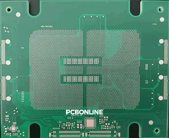
3. High-Density Storage & Memory
HDI PCBs support micro-BGA or CSP stacked microvias, connecting HBM to the GPU. They are used in:
- HBM/HBM2E/HBM3
- High-bandwidth memory adjacent to GPUs/AI chips
4. AI Edge Devices & High-Speed Industrial Control
HDI PCBs reduce size while maintaining high-speed I/O. High-frequency, high-density routing requires HDI technology. HDI PCBs are used in:
- AI inference accelerator cards (Edge)
- Small GPU/FPGA accelerator boards
- High-speed industrial control
- High-speed sensor acquisition and FPGA/MCU integration
5. Other AI Hardware Applications
- PCIe Gen5/6 expansion cards (AI/FPGA/SSD accelerators)
- Custom ASIC accelerators
- 5G/6G base station boards
- High-performance embedded GPU/AI SoC carrier boards
![]()
To sum up, in AI hardware, high-density interconnect PCBs are used for:
- High-performance GPU / FPGA / ASIC carrier boards (≥24 layers, microvias)
- High-speed networking and data center switch boards
- High-bandwidth memory (HBM) interfaces
- Edge AI inference / industrial control boards
- High-speed expansion cards/communication base stations
Partner with PCBONLINE for Turnkey HDI PCBs for AI, High-Speed Network, and BGA Devices
If you are designing any AI servers, high-speed network equipment, accelerators, etc, work with PCBONLINE for turnkey HDI PCB service. We provide high-density interconnect PCB manufacturing services that cover GPU/FPGA/BGA/IC package substrate PCB manufacturing, assembly, testing, and reliability assurance.
Founded in 2005, PBONLINE has two large advanced PCB manufacturing bases and one PCB assembly factory.
PCBONLINE has strong HDI PCB fabrication capabilities from 4 to 64 layers, meeting your HDI PCB demands from the initial idea to high-volume production.
HDI PCBs 1+N+1, 2+N+2, 3+N+3, and 4+N+4 can be manufactured, and microvias can be in any layer in R&D, with microvia structures of 100 µm and 125 µm.
We provide one-stop HDI PCB manufacturing, including component sourcing, PCB fabrication, assembly, testing, and system integration using any GPU, FPGA, ASIC, or CPU.
SMT assembly with down to 0.35mm fine-pitch BGA placement accuracy and custom reflow profiles for warpage-free soldering.
100% X-Ray inspection, functional testing, and burn-in testing for guaranteed reliability.
We have rich experience in impedance control, oven temperature control, and assembly fixture designs.
High-quality HDI PCBA manufacturing certified with ISO 9001:2015, ISO 14001:2015, IATF 16949:2016, RoHS, REACH, UL, and IPC-A-610 Class 2/3.
At PCBONLINE, we can help our clients reduce costs while achieving the highest levels of performance and reliability. If you feel interested in HDI PCBs for AI hardware, network equipment, etc, send your inquiry by email to info@pcbonline.com.
Conclusion
High-density interconnect PCBs feature microvias, buried/blind via, and high routing density. HDI PCBs are used for AI servers, high-performance computing, high-speed network equipment, communication base stations, HBM interfaces, etc. If you are looking for a trusted partner for these applications, contact PCBONLINE for turnkey OEM HDI PCB manufacturing.
PCB fabrication at PCBONLINE.pdf


