
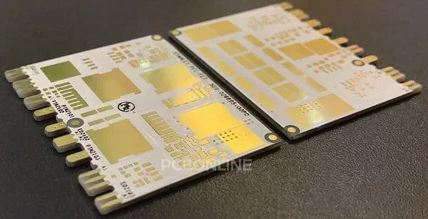
Thin film and thick film are two indispensable manufacturing technologies for ceramic PCBs (printed circuit boards) to meet specialized requirements. Thin-film PCBs can provide the finest circuits with a minimum trace width/space of 5µm to 20µm. Thick-film PCBs, by contrast, have the least precise circuits among all ceramic PCBs, but they are the only ones that can silkscreen print resistors, capacitors, or dielectric layers for hybrid circuits during PCB manufacturing.
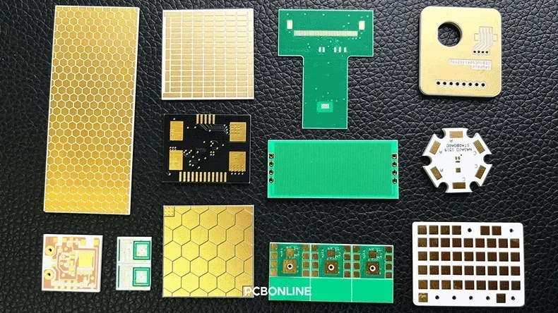
PCBONLINE provides high-quality and one-stop ceramic PCB manufacturing and assembly to final devices. In our article, you can learn about ceramic thin-film and thick-film PCBs, including what they have in common and how they differ.
Thin Film PCB
Thin-film PCBs are precision ceramic PCBs used for RF and microelectronic applications. The thin-film technology uses a high-vacuum deposition method, which is adapted from semiconductor fabrication. Thin-film PCBs offer the highest feature resolution of ceramic PCBs and excellent electrical performance.
Thin-film PCBs use stacked multi-metal, including:
- Ti and Cr, which form the adhesion layer to bond the metal firmly to the substrate.
- Pt-Pd-Mo-W, which forms the barrier layer for thermal resistance and impedance control.
- Au as the interconnect with low resistance and strong anti-oxidation.
- Ni as the barrier layer beneath the Au layer or as the soldering pads.
During thin-film PCB manufacturing, the ceramic substrate is placed in a vacuum chamber, and metal layers are deposited using physical vapor deposition, sputtering, or evaporation. The deposited metal layer is pure and uniform.
Next, a photoresist layer is applied, exposed through a precise mask, and developed to define the circuit pattern.
Then the exposed metal is selectively etched away or used as a seed layer for electrochemical plating to build up the final desired thickness.
Finally, remove the excess seed layer and get the desired circuit pattern.
Characteristics of thin-film PCBs are —
- Highly controllable and thin trace thickness of 0.5µm to 10µm.
- Fine circuit pattern definition with sub-10µm line widths and complex routing due to the photolithography process.
- Thin-film PCBs offer superior electrical conductivity, low surface roughness, and high film uniformity, as metal adhesion is based on direct chemical/physical bonding to the ceramic.
- Thin-film PCBs have minimal loss tangent and high dimensional precision for impedance control. This meets high-frequency application requirements, so thin-film ceramic PCBs are used for RF and high-frequency devices.
Thick Film PCB
Thick-film PCBs are cost-effective ceramic PCBs. Thick film technology uses screen printing to deposit conductive, resistive, and dielectric pastes onto ceramic. It is used for volume manufacturing.
The ceramic substrate of the PCB is already sintered and rigid, while the other materials are viscous and paste-like compositions before sintering. The paste materials used in thick-film PCB manufacturing include:
- Metal pastes (Ag, Ag-Pd, or Pt-Au) form the circuit traces and PCB pads of the thick-film PCB and electrodes of the thick-film capacitors.
- RuO₂ resistor pastes (sometimes, Pb-Ru-glass or metal-glass composite), which act as resistors of the PCB and achieve precise resistance through laser trimming.
- Glass-ceramic dielectric pastes, which form the dielectric layer for stacking and capacitor electrodes. The dielectric layer provides adhesion, ensuring metals are firmly sintered onto the ceramic substrate.
- Organic binder/vehicle, which provides viscosity to the pastes and will evaporate when drying.
Before thick-film PCB manufacturing, we had already fabricated a stencil for silkscreen printing.
During thick-film PCB manufacturing, the PCB material pastes go through the openings of the stencil to silkscreen print onto the ceramic substrate.
Next, the organic vehicle is evaporated at low temperatures (<150°C), and the functional pastes are solidified to prevent flow for sintering.
Finally is the sintering step at temperatures of 850°C to 1000°C. The metal particles are sintered and densified, while the glass-ceramic powders melt and adhere to the ceramic substrate.
After sintering, the metal layer solidifies with strong adhesion, resistive materials form a stable resistive film, and the dielectric layer forms a dense insulating layer.
Characteristics of thick-film PCBs are —
- Thick trace thickness of 10µm to 25µm.
- The least refined circuit with minimum line widths and spacings of 100µm to 150µm. This is because the physical limits of the screen print stencil constrain the feature resolution.
- Good mechanical strength as the circuit adhesion is achieved through glass-ceramic bonding.
- Higher trace resistivity than pure bulk metal due to residual glass and porous microstructure.
- Achieving component integration and multilayer dielectrics during PCB manufacturing by printing integrated resistors and capacitors using pastes
Thin-Film PCB vs Thick-Film PCB
Here, we explain what thin-film and thick-film PCBs have in common and how they differ.
What thin-film and thick-film PCBs have in common
From the above descriptions of thin-film and thick-film PCBs, you can see that both are single-layer ceramic PCB technologies, and their ceramic substrate is already rigid and sintered before PCB fabrication.
Besides, what thin-film and thick-film PCBs have in common are also all the ceramic PCBs have:
- High thermal conductivity enables efficient heat spreading away from active devices.
- Low coefficient of thermal expansion, excellent mechanical matching with silicon, minimizing stress at the component interface.
- Dimensional stability with high tolerance to thermal cycling and process temperatures.
How thin-film and thick-film PCBs differ
The difference between thin-film and thick-film PCB fabrication lies in how the metal layer is applied and patterned. The distinction between thin-film and thick-film PCBs lies in their circuit precision, and thick-film PCBs integrate capacitors and resistors during manufacturing.
|
Feature
|
Thin film PCB
|
Thick film PCB
|
|
Deposition method
|
PVD, sputtering, or electroplating
|
Screen printing
|
|
Trace thickness
|
0.5µm to 10µm (high purity)
|
10µm to 25µm (composite paste)
|
|
Minimum line width
|
<20µm (high resolution)
|
>100µm (low resolution)
|
|
Surface smoothness
|
Excellent (low RF loss)
|
Moderate (higher RF loss)
|
|
Metallization
|
Ti/Ni/Au, Cr/Au, Pure Cu (plated)
|
Ag, Au, Pd/Ag, Cu (paste)
|
|
Cost
|
High (vacuum, cleanroom intensive)
|
Low (batch/volume processing)
|
|
Application
|
RF/microwave, high-speed sensors, IC packaging
|
Hybrid circuits, resistor networks, power/LED lighting
|
Based on the applications, choose thin-film PCBs when:
- The circuit operates at GHz frequencies where trace loss must be minimized.
- High component density demands line widths under 50µm.
- Tight impedance control and high-precision features are mandatory.
Choose thick-film PCBs when:
- Cost-efficiency in high volume is the priority.
- The circuit only requires moderate feature resolution >100µm.
- Integrated passive components, especially resistors, need to be formed directly on the substrate.
To sum up, thin-film PCBs enable the integration required for advanced microelectronics, while thick-film PCBs remain the workhorse for robust, high-temperature, and cost-optimized hybrid systems.
PCBONLINE: High-Quality Ceramic PCB Board Manufacturer
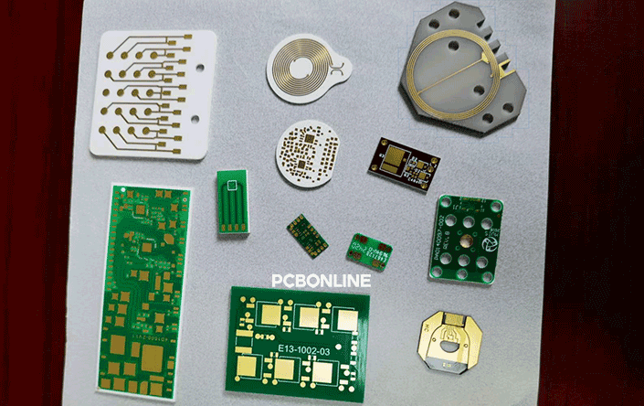
PCBONLINE is a one-stop ceramic PCB board manufacturer founded in 2005, providing turnkey AlN PCB and alumina PCB made by any of the above manufacturing methods. Besides, ceramic IGBT modules, ceramic COB LED modules, ceramic LED plates, etc, can also be provided by PCBONLINE.
PCBONLINE manufactures, assembles, and tests ceramic PCBs as a source factory manufacturer under one roof, from prototypes to bulky production.
PCBONLINE can manufacture ceramic PCBs to be HDI, high-frequency, multilayer, and double-sided.
Provides one-on-one free and professional DFM (design for manufacturing) for ceramic PCB boards before and during prototyping/sampling to ensure the success of your project and seamless mass production.
PCBONLINE has powerful ceramic PCB manufacturing capabilities. The copper layer thickness of ceramic PCBs is arbitrarily customized from 1μm to 1mm.
High-quality ceramic PCB boards with no oxide layer on the PCB surface have better welding performance and high-temperature resistance.
For ceramic PCB manufacturing and assembly orders at $5,000 and above, we offer free complete ceramic PCBA samples and functional tests. If you feel interested in ceramic PCB boards from PCBONLINE, feel free to send your inquiry by email at info@pcbonline.com.
Conclusion
Thin-film and thick-film PCBs are both single-layer ceramic PCBs. Thin-film PCBs offer precise circuits and are ideal for RF and high-frequency applications. Thick-film PCBs integrate resistors and capacitors during manufacturing. PCBONLINE provides high-quality ceramic PCB manufacturing. To ensure the success of your ceramic PCB/PCBA projects, work with the turnkey ceramic PCB manufacturer PCBONLINE.
PCB assembly at PCBONLINE.pdf
PCB fabrication at PCBONLINE.pdf


