
Surface Mount Technology (SMT) has dominated printed circuit board (PCB) assembly in electronics manufacturing, allowing for smaller, faster, and more efficient electronic devices. PCBONLINE provides one-stop PCB assembly services from prototypes to mass production for mid and high-end applications, and we have rich experience in the SMT surface mount technology. Our article explains SMT surface mount technology, its step-by-step process, common component types, the difference between SMT and SMD, and its benefits and drawbacks.
What is Surface Mount Technology (SMT)?
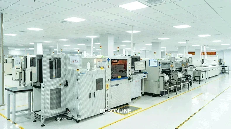
At PCBONLINE, our SMT assembly process is fully automated and precise. We ensure efficient and high-quality PCB production. The steps of the SMT surface mount technology process are below.
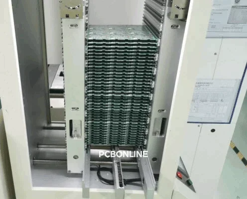
Loading bare PCBs
The process starts by loading bare PCBs onto the SMT production line. A dedicated loader machine feeds individual PCBs automatically. This ensures a continuous flow.
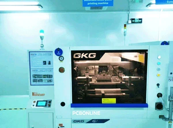
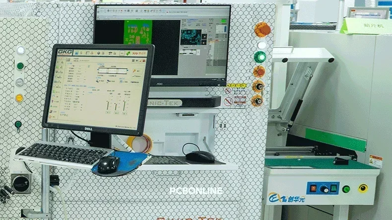
Solder paste printing
Next, the PCB moves to the solder paste printing station. A vision system precisely aligns the PCB under an SMT stencil. A squeegee then moves across the stencil. It presses a precise amount of solder paste through the stencil's openings. This paste goes onto the designated pads on the PCB surface. Solder paste is a sticky mix of tiny solder particles and flux. It acts as a temporary adhesive and forms a strong electrical connection. The squeegee's controlled speed, pressure, and angle are vital for consistent application.
Solder paste inspection (SPI)
After printing, the PCB undergoes Solder Paste Inspection (SPI). A 3D SPI machine scans the applied solder paste using an infrared camera. This inspection verifies the paste's position, shape, and thickness against quality standards. Deviations are caught early. This prevents costly rework later in the process.
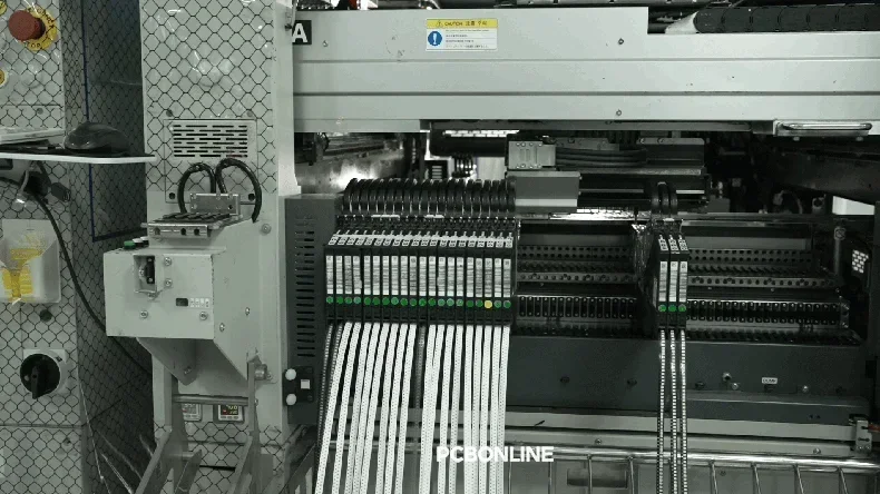
Pick-and-place of SMDs
Following a successful SPI, the PCB goes to the pick-and-place stage. High-speed, automated machines use vacuum nozzles or grippers. They accurately pick individual Surface Mount Devices (SMDs) from feeders. Advanced vision systems then precisely place each component. It goes onto its corresponding solder-pasted pads on the PCB. Modern pick-and-place machines can place tens of thousands of components per hour. This highlights SMT's incredible efficiency.
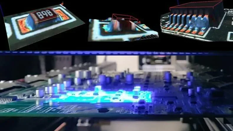
Automated optical inspection (AOI) before reflow soldering
Before reflow soldering, another critical inspection occurs. A 3D Automated Optical Inspection (AOI) machine is used. This AOI checks the populated PCBA for placement issues. It looks for missing components, misalignment, or incorrect polarity. Catching these errors early allows for immediate correction. This prevents permanently flawed assemblies.
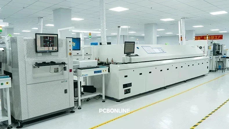
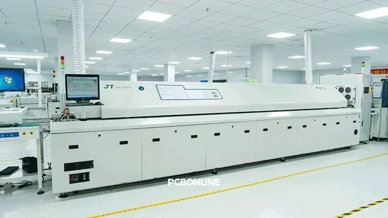
Reflow soldering
The PCBA then enters a reflow oven. This is typically a lead-free oven with multiple temperature zones. As the board moves through these zones, it undergoes a careful heating profile. The solder paste first melts (reflows). The molten solder then creates strong metallurgical bonds between the SMD leads/pads and the PCB pads. The molten solder's surface tension helps self-align components. Finally, the board cools. The solder solidifies, forming permanent electrical and mechanical connections.
Automated optical inspection (AOI) after reflow
The final major step is AOI after reflow. A 3D AOI machine performs a full scan of the soldered board. It ensures soldering quality and component placement accuracy. This inspection checks for common defects. These include solder bridging, tombstoning, and irregular solder joint shapes. This final quality check ensures the assembled PCB meets strict standards.
Types of Surface-Mounted Components
The components used in SMT are called surface mount devices (SMDs). They are compact with leads or contacts specifically for surface mounting. Key SMD types include:
- SMD resistors: These passive components limit electrical currents and dissipate heat. Common types include ordinary resistors, shunt resistors, wirewound resistors, and metal film resistors. They are usually small, rectangular chips with metallic end caps.
- SMD capacitors: Also passive, SMD capacitors store electrical energy. They block direct current (DC) and allow alternating current (AC) to pass. Ceramic, tantalum, and aluminum electrolytic capacitors are widely used. They vary in size and capacitance.
- SMD inductors: These components convert electrical energy into magnetic energy. They are used for filtering, energy storage, and impedance matching. Common types include inductor coils and choke coils.
- SMD diodes: Diodes are semiconductor devices. They allow current to flow in one direction. They are often used for AC to DC conversion, signal rectification, and voltage regulation. Types include ordinary diodes, two-terminal diodes, and Light-Emitting Diodes (LEDs).
- SMD transistors: These semiconductor devices amplify or switch electronic signals and power. Phototransistors are a specific type of SMD transistor that responds to light.
- ICs (Integrated Circuits): ICs are miniature electronic circuits on a semiconductor material. They come in various surface-mount packages. Examples include SOP, QFP, SOJ, PLCC, BGA, and CSP. These packages differ in pin count, size, and thermal dissipation.
- SMD crystal oscillators: Also known as quartz crystals, these provide a stable base frequency and clock signals. They are essential for digital circuits and microcontrollers.
- Other SMDs include SMD resistor banks, SMD switches, SMD magnetic beads (for noise suppression), SMD heat sinks, and SMD transformers.
On a PCB assembly or PCBA, you will notice that each surface mount component takes a land pattern on the board. We call it an SMD footprint, which is the dimension of a copper pad where an SMD component is soldered. Each type and size of SMD has a specific footprint design.
Smaller footprints allow for greater component density and miniaturization. PCBONLINE provides fine-pitch PCB assembly for PCBs requiring small-footprint SMDs.
Here's a table of common SMD footprint sizes.
|
Footprint name (imperial)
|
Metric code (L x W in mm)
|
Dimensions (″) L x W
|
Dimensions (mm) L x W
|
Typical application
|
|
01005
|
0402
|
0.016 x 0.008
|
0.4 x 0.2
|
Ultra-compact devices, wearables
|
|
0201
|
0603
|
0.024 x 0.012
|
0.6 x 0.3
|
Smartphones, portable electronics
|
|
0402
|
1005
|
0.040 x 0.020
|
1.0 x 0.5
|
Common in consumer electronics
|
|
0603
|
1608
|
0.063 x 0.031
|
1.6 x 0.8
|
Widely used, good balance of size/power
|
|
0805
|
2012
|
0.079 x 0.049
|
2.0 x 1.25
|
General purpose, less critical density
|
|
1206
|
3216
|
0.126 x 0.063
|
3.2 x 1.6
|
Higher power, less dense applications
|
Difference Between SMT and SMD
The terms SMT and SMD are often confused by beginners. However, they have distinct meanings:
SMT (Surface Mount Technology): SMT refers to the entire method of mounting components onto a PCB surface. It includes the complete process, requiring the equipment, techniques, and procedures used in the assembly line (like solder paste printing, pick-and-place, and reflow soldering).
SMD (Surface Mount Device): SMD refers to the electronic components used in SMT assembly. These parts (resistors, capacitors, ICs, etc.) are designed to be mounted on the PCB surface. They are the physical items picked and placed during SMT.
In short, SMT is the "how" (the technology/process). SMD is the "what" (the component). SMDs were developed to take advantage of SMT. SMT relies on available SMDs to function.
Pros and Cons of SMT Surface Mount Technology
SMT offers significant benefits over THT. However, it also has some challenges.
Pros of SMT
- Higher component density: SMT allows components to be packed closer. They can be placed on both sides of the PCB. This eliminates drilled holes. The result is smaller, lighter, and more compact devices. This is vital for portable electronics.
- Faster assembly: The SMT process is highly automated. Pick-and-place machines work quickly. This means significantly faster production and lower labor costs.
- Improved electrical performance: SMDs have shorter or no leads. This reduces unwanted inductance and capacitance. It leads to better high-frequency performance and improved signal integrity. It also reduces electromagnetic interference (EMI).
- Cost-effective for mass production: While initial equipment costs are high, SMT lowers overall manufacturing costs for large volumes. This is due to less material handling, fewer drilling, and higher efficiency. SMT components can also be less expensive.
- Enhanced mechanical performance: SMDs are more resistant to shock and vibration. This is due to their lower mass and tight connection to the PCB.
- Automatic placement correction: During reflow, molten solder's surface tension can self-align slightly misaligned components. This improves assembly accuracy.
- Design flexibility: SMT allows for more complex circuit designs. It also enables the use of more PCB layers.
Cons of SMT
- High initial investment: Setting up an SMT line requires expensive, specialized equipment. This includes reflow ovens, pick-and-place machines, and solder paste printers. This can be a barrier for small manufacturers. PCBONLINE has worked for 20 years in SMT assembly. We have 4 complete SMT lines for your manufacturing needs.
- Thermal sensitivity: Many SMDs are sensitive to temperature changes during reflow. Precise control of the oven's temperature profile is critical to prevent component damage. PCBONLINE has rich experience in reflow oven temperature control.
- Solder joint inspection challenges: Inspecting solder joints can be difficult, especially for packages like BGAs. These have connections underneath the component. X-ray inspection is required. For hidden-joint components like BGAs, PCBONLINE conducts an X-ray inspection after the SMT process to ensure quality.
- Susceptibility to mechanical stress: Solder joints for some SMDs might be less mechanically robust than through-hole connections. This applies to larger or heavier components under significant physical stress.
- Not ideal for high-power components: Some very large, high-power, and high-voltage components still should use THT technology to insert into the drilled holes for THT assembly. This is due to their strength or heat dissipation needs.
Partner with PCBONLINE for SMT Assembly
PCBONLINE not only provides SMT assembly but also THT assembly and box-build assembly.
PCBONLINE handles the entire PCB assembly process, from component procurement, SMT and THT assembly, to enclosures and final product packaging.
Founded in 2005, PCBONLINE has two advanced PCB manufacturing bases in Jiangsu and Jiangxi Provinces, one turnkey PCB assembly factory in Shenzhen for PCBA and box builds. We also have an R&D team.

We provide one-on-one free and professional DFM before and during prototyping/sampling, to ensure the manufacturability and project success.
Each SMT line at PCBONLINE is equipped with three advanced pick-and-place machines, supporting up to 376 SMD placements per PCB, enabling us to surface mount high-density and fine-pitch PCBs.
Powerful manufacturing capabilities in SMT surface mount technology, including 3D SPI, 3D pre- and post-reflow AOI, X-ray inspection, and first-article inspection.
PCBONLINE provides PCBAs and box builds as a source factory manufacturer under one roof, from prototypes to bulky production, saving costs and time for you.
High-quality PCBA manufacturing certified with ISO 9001:2015, ISO 14001:2015, IATF 16949:2016, RoHS, REACH, UL, and IPC-A-610 Class 2/3.
PCBONLINE has rich experience in reflow oven temperature control and offers improvement suggestions for your design if any optimization.
When your PCBA project enters mass production, we refund the fees for prototypes and offer free PCBA functional testing.
Whether you need SMT assembly for communications, consumer, automotive, medical, or industrial applications, we have the equipment, experience, and capabilities to deliver superior results for you in one stop. To get a quote for PCB and SMT manufacturing, email us at info@pcbonline.com.
Conclusion
SMT surface mount technology enables miniaturization, efficiency, and high performance of modern electronic devices. PCBONLINE provides high-quality SMT PCBA manufacturing. To ensure the manufacturing success of your PCBA project, partner with the turnkey PCBA manufacturer PCBONLINE.
PCB assembly at PCBONLINE.pdf


