
Reflow soldering is a soldering process used in electronic assembly, mainly used to fix surface mount components (SMD) on printed circuit boards (PCB). It is a necessary step in surface mount technology (SMT), but whether it is necessary depends on the specific process requirements. In mainstream SMT production, reflow soldering is an essential core process; there may be alternatives in special scenarios, but they all have obvious limitations. Therefore, this blog will explore various details about the reflow soldering process.
In this article:
Part 1. What is reflow soldering and why need it? Part 2. Specific Process Part 3. Common Errors in Reflow OvenWhat is reflow soldering and why need it?
Reflow soldering precisely controls the temperature curve, so that the solder paste goes through four stages: preheating, wetting, reflow and cooling, and finally achieves metallurgical bonding between component pins and PCB pads. It is suitable for high-density and miniaturized circuit assembly.
Specific Process
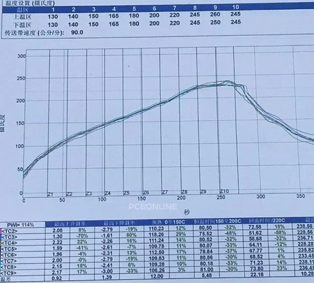
Reflow soldering is usually divided into four main stages, each of which is critical to soldering quality and component reliability. The following is a detailed division of the stages and their functions:
Preheat:
The preheating stage is the starting point of the whole process, and its core is to gradually heat the circuit board from room temperature to about 150°C. In this stage, the heating rate must be strictly controlled (usually 1-3°C/second) to avoid thermal stress damage to components due to sudden temperature rise or splashing caused by violent evaporation of volatile solvents in the solder paste. At the same time, slow heating allows the low-boiling point components in the solder paste to fully volatilize, reducing the problem of solder joint bubbles or voids caused by residual gas in the subsequent welding process, laying the foundation for the subsequent stages.
Soak:
The soak stage is usually maintained in the temperature range of 150-180°C for 60-120 seconds. The core function of this stage is to activate the chemical properties of the flux, so that it can effectively remove the oxide layer on the surface of the pad and the component pin, creating conditions for the combination of molten solder and the metal surface. In addition, the soak process ensures that the temperature distribution of the entire circuit board tends to be uniform, avoiding poor soldering in some areas or component offset due to local temperature differences, which is especially important for multi-layer boards with large differences in thermal capacity or dense component layouts.
Reflow:
The reflow stage is the core step of soldering. The temperature rises rapidly to the peak value (lead-free solder paste usually needs to reach 235-250°C) and is maintained at this high temperature for 30-60 seconds. When the temperature exceeds the melting point of the solder (such as 217°C for SnAgCu alloy), the solder paste completely melts into liquid, wets and spreads on the metal surface to form intermetallic compounds (IMC), thereby achieving reliable electrical and mechanical connections. The surface tension of liquid solder also produces a "self-correction" effect on slightly offset components, improving mounting accuracy. Temperature control at this stage needs to balance sufficient melting with avoiding overheating and damage to sensitive components.
Cooling:
During the cooling stage, the solder joints are solidified and fixed by a controllable cooling rate (usually 1-4°C/second). Too fast cooling may cause coarse grains or microcracks inside the solder joints, affecting the mechanical strength; while too slow cooling may aggravate the thermal damage to the components and substrates caused by high temperature. The ideal cooling curve can form a dense microstructure of the solder joints, while ensuring the compatibility of the components and PCB materials under the difference in thermal expansion coefficients, and ultimately achieve a high-reliability welding result. The success of the entire process depends on the fine control of the temperature curve, which needs to be dynamically optimized in combination with the characteristics of the solder paste, the heat resistance limit of the components and the complexity of the PCB design.
Common Errors in Reflow Oven
Solder Joint Oxidation
The surface of the solder joint is dark, without metallic luster, and the wettability is reduced. The main reason is that the solder joint is exposed to the air for a long time at high temperature, resulting in a slow cooling rate. At the same time, the oxygen content in the reflow furnace is high, which eventually leads to solder oxidation.
Voiding
Insufficient evaporation of solvent or flux during the preheating stage, coupled with the failure of gas to escape from the molten solder during reflow, causes bubbles or voids to exist inside the solder joint, affecting thermal conductivity and mechanical strength.
Cold Solder Joint
The solder is not completely melted and cannot form an effective intermetallic compound (IMC); the heat capacity of the component or pad is large, resulting in the local temperature not reaching the melting point. Therefore, the surface of the finished solder joint is rough, matte, grayish, with low mechanical strength and easy to break.
Non-Wetting
Some solder pads or pin oxide layers are not effectively removed by the flux, and the flux is not active enough due to insufficient time or too low temperature during the constant temperature stage. The solder fails to wet the solder pad or component pin, and the solder joint separates from the metal surface.
There are many problems in the actual operation of reflow oven, which requires a manufacturer's production experience and engineering management capabilities. Therefore, you need to consider whether the manufacturer has good quality management capabilities to choose a suitable PCB manufacturer.
One-Stop HDI PCB Manufacturer and Its PCB Via Filing Capabilities
If you're looking for turnkey HDI electronics manufacturing services (EMS) from hardware development to PCBA fabrication and box-build assembly, you can work with the one-stop HDI PCBA manufacturer PCBONLINE.
Founded in 1999, PCBONLINE has R&D capabilities for HDI projects and EMS manufacturing capabilities, including via filling for stacked vias. It provides 4-to-64-layer HDI PCB fabrication, assembly, and PCBA box-build assembly. You can order various HDI PCBs from PCBONLINE, such as FR4, polyimide (flexible PCB), polyimide + FR4 (rigid-flex PCB), and PTFE/Rogers (high-frequency PCB).

3000m² of production capacity per day for HDI PCBs with builds of 1+N+1, 2+N+2, 3+N+3,4+N+4, and arbitrary interconnection in any layers.
PCBONLINE has hardware and software R&D capabilities for IoT applications requiring HDI design, including PCBA and enclosures.
We can manufacture complex PCBs with stacker vias, via-in-pad, microvias, inlay boards, heavy copper designs, and hybrid and fine structure lay-ups.
Besides HDI PCB fabrication, we have powerful capabilities in fine-pitch assembly for HDI PCB assembly.
We have rich R&D and manufacturing experience for HDI applications such as FPGA boards.
High-quality HDI PCB and PCBA manufacturing certified with ISO 9001:2015, IATF 16949, RoHS, REACH, UL, and IPC-A-610 Class 2/3.
Here'e the PCB via filing capabilities at PCBONLINEL:
- Micriavia filling with copper: laser via size 0.1-0.125mm, priority 0.1mm
- Finished hole size for via-in-pad filling with resin: 0.1-0.9mm (drill size 0.15-1.0mm), 0.3-0.55mm normal (drill size 0.4-0.65mm)
- Max aspect ratio for via-in-pad filling with resin PCB - 12: 1
- Min resin plugged PCB thickness: 0.2mm
- Max via-filling ith resin PCB thickness: 3.2mm
- Making different hole sizes with via filling in one board: Yes
- Via filling with copper/silver: Yes
If you need HDI PCBAs or any other PCBAs requiring via filling, please send your email to PCBONLINE at info@pcbonline.com. We will provide one-on-one engineering support to you.
Conclusion
Via filling is used for creating stacked vias in HDI PCB fabrication, BGA/CSP/QFN IC packaging, and filling PCB via-in-pad with resin during multilayer PCB fabrication. If you need one-stop electronics manufacturing for your HDI PCBA project, contact the one-stop advanced PCB manufacturer PCBONLINE for high-quality PCBA and box-build solutions tailored to your project's needs.
PCB fabrication at PCBONLINE.pdf


