
In HDI PCB (high-density-interconnect printed circuit board) fabrication, sometimes, the via tenting step is required for these purposes:
- Preventing the solder paste from going in the PCB vias during PCB assembly.
- Ensuring flatness of the PCB vias for soldering.
- Improving signal integrity by sealing the hole opening to reduce crosstalk and reflection.
What is via tenting? When to apply single-sided or double-sided via tenting on the PCB? Learn about PCB via tenting from this blog by the author Zbigniew Huber. You can also visit his website at https://www.superengineer.net/ for more knowledge about electronics engineering.
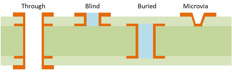
What is a PCB Via?
PCBs contain numerous electrical connections between internal and external copper tracks. These connections are created by copper-plated holes known as vias.
The IPC-T-50 standard defines a PCB via as: "A plated hole that is used as an interlayer connection but is not intended for inserting a component lead or metallic part."
Via Tenting
In HDI PCB, the holes can increase EMI and affect signal integrity, so it's better to cover the PCB vias with solder masks. PCB designers may find it helpful to cover through vias with a solder mask material called via tenting.
Via tenting can prevent solder wicking from nearby solder lands. It can be useful when solder lands are very close to the via opening and the solder mask "dam" is insufficient to prevent solder flow.
It also protects the via plating from contaminants. Various contaminants may enter the via barrel during circuit board assembly (i.e., flux) or field use. Such issues may lead to corrosion in some circumstances and reduce the PCB's reliability.
Besides, PCB via tenting is cost-effective. The tenting process with the same solder mask used over the board surface incurs no additional processing cost.
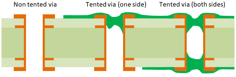
Via tenting on only one side or both sides? And the via tenting should be partial or full on the hole? Below are the answers.
Reason for One-side vs Two Sides: Reliability Concerns
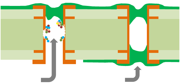
If the solder mask covering the via is cracked, incomplete, or open on one side (one side tenting), this might lead to reduced board reliability due to corrosion.
Various contaminants may enter the via through the opening. Then the contaminants may be trapped in the barrel and over time cause corrosion of the copper plating. Finally, it may lead to electrical connection failure. These contaminants may originate from the PCB manufacturing process, from the soldering process (ie. Flux residues), or from the environment during the device's operation.
If the via tenting method is considered, then double-sided tenting is recommended in most cases.
To ensure full coverage of the via barrel with the solder mask, use an adequate (small) diameter via, typically 0.3mm or less. Consult the PCB manufacturer to fully understand the limits of the used LPI (Liquid Photo Imageable) solder mask and follow the recommendations.
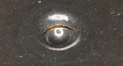
If the via opening is too large, then the tenting may be incomplete or may crack, leaving a small gap, an opening, through which contaminants could enter inside. In some cases, such conditions may cause corrosion. Example photo of tenting crack:
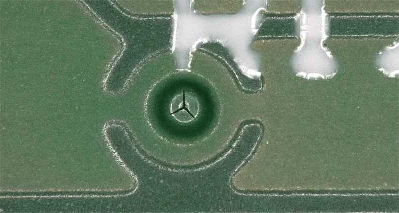
Tenting crack with via copper plating visible:
Another reliability concern may arise when double-sided tented via is used and large air bubbles/moisture is entrapped inside. If the PCB board is then subjected to significant temperature changes, the entrapped air bubble expands and may lead to a tenting crack or even via plating crack.
For high-reliability applications, consider other via protection methods, like epoxy filling. Get familiar with filled-via types, some of which provide complete barrel protection with a dielectric material. Filled vias provide robust protection against contamination from the assembly process or the field and eliminate the risk of entrapped air inside the barrel.
To Sum up
Via tenting is a cost-effective and easy-to-implement solution. It may help reduce solder wicking from nearby solder lands and limit contamination entrapment. However, when single-side via tenting is used, it may allow chemicals to entrap and cause the corrosion of the via plating, finally leading to electrical connection failure. Use of one-side tenting should be limited to specific applications like additional heat transfer from power devices, connection to power plane, etc.
If tenting of the via is considered, I recommend using double-sided tenting. Always consult your PCB manufacturer PCBONLINE regarding the maximum via hole size to ensure reliable tenting. Typically, 0.3mm or less via diameter provides repeatable coverage.
For high-reliability applications, via tenting is not a good idea due to the following:
- The tenting may crack and create an opening for contamination, leading to via plating corrosion.
- Double-sided sealed tenting may entrap air bubbles/moisture inside. During thermal processes or thermal cycling, the air bubble/moisture expands and increases the risk of via crack or tenting crack.
When designing a board for high-reliability applications use standard vias (the barrel is uncovered) or consider other solutions like epoxy filling. In the latter case, the via barrel is fully protected against harsh environments. See IPC-4761 for more details.
PCB fabrication at PCBONLINE.pdf


