For flexible PCBs, PTFE PCBs, FR4 PCBs, and ceramic PCBs, laser drilling can be applied in their fabrication process to drill accurate and tiny holes. Laser drilling is critical, especially for HDI (high-density interconnect) PCBs, and directly affects high-speed signal stability and product reliability.
In this blog, you can understand PCB laser drilling easily and comprehensively, including what it is, its difference from mechanical drills, the PCB laser-drilled holes, and laser drilling costs.
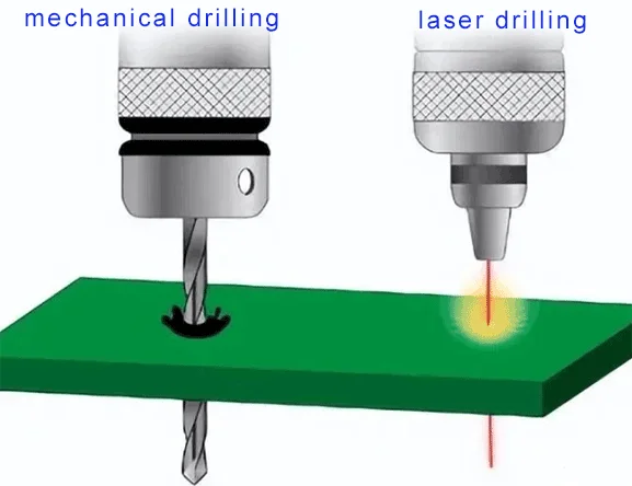
PCB Laser Drilling vs Mechanical Drilling
Laser drilling is a digital-controlled technology that drills microvias to connect different PCB layers. The PCB laser drilling methods include CO2 laser drilling and UV laser drilling.

What PCB drilling method should be used for your PCB board? It depends on the hole aperture you design:
- Mechanical drilling for PCB holes of 150μm (0.15mm) and above
- CO2 laser drilling for PCB holes between 150μm and 100μm (0.1mm-0.15mm)
- UV laser drilling for PCB holes below 100μm (0.1mm)
From the above, you may know the aperture ranges of mechanical drilling and laser drilling. Mechanical drilling drills through holes of 0.15mm and above.
Laser drilling drills microvias with the aperture below 0.15mm.
Below are more details on PCB mechanical drilling vs. laser drilling.
1. Mechanical drilling
The inner diameter of the holes by mechanical drilling is above 0.2 mm.
PCBONLINE, an advanced PCB manufacturer, can make the minimum mechanical holes of 0.15mm.
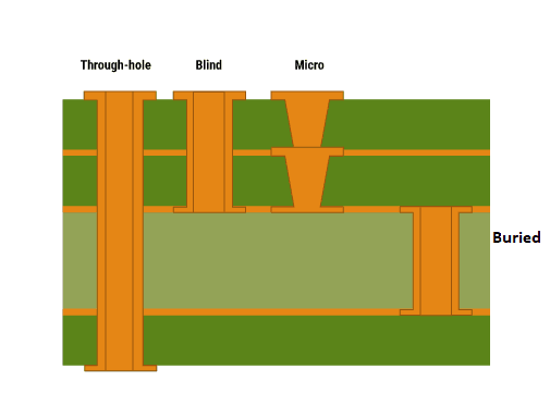
Mechanical drilling goes through the PCB board or all the layers to be drilled.
2. Laser drilling
The inner diameter of laser-drilled holes - microvias, is generally 0.1mm.
Because of energy loss during drilling, it can't directly penetrate a multi-layer PCB but only one PCB layer each time. So it is usually used in blind hole PCBs.
In addition, due to energy loss during drilling, the microvia diameter is in the shape of an inverted trapezoid. Its aspect ratio is typically 0.75:1.
Compared with mechanical drilling, laser drilling has a higher resolution and smaller processing aperture. Besides, because the laser head does not touch the PCB, there is no PCB material damage by mechanical vibrations.
Now, you know laser drilling and its differences from mechanical drilling. You may still feel puzzled by the different PCB holes drilled by laser and mechanical drilling. Let's clarify the PCB holes easily below.
What Holes Are Drilled by PCB Laser Drilling

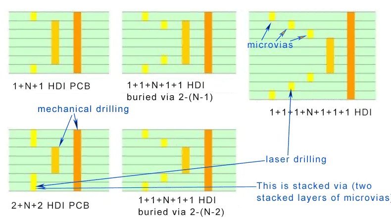
The above image shows the PCB holes in HDI PCBs of different stack-ups.
The PCB holes in the yellow color are in the outer layers, they are micorvias that are laser drilled. They typically have a 0.75 aspect ratio through the aspect ratio range falls in 0.5-1.
The PCB holes in the dark orange color penetrate the PCB, they are through holes (PTH). The PCB holes in the tangerine yellow color are in the inner layers, they are buried vias. Both of them are mechanically drilled.
Note: In the 2+N+2 HDI PCB stack-up, 2 means two layers of microvias are stacked to form a stacked via. In contrast, a staggered via is formed by two or more microvias that are staggered.
So now we can answer the question of what holes are drilled by PCB laser drilling. The single microvias, stacked vias, and staggered vias are drilled by laser.
Facts about PCB Laser Drilling Cost
Is PCB laser drilling more costly than mechanical drilling? Yes. That's why HDI PCBs are more expensive than mechanically-drilled PCBs made of the same substrate materials.
Here are some facts about PCB drilling costs corresponding to the PCB via design:
①. The smaller the aperture, the smaller the drill bit, so the higher the price of the small drill bit, and the higher the requirements for the PCB factory.
②. The PCB with laser holes is about 30% more expensive than those without laser holes in the same materials. The more layers with laser holes, the higher the cost.
③. The more complicated the PCB via drilling process, the higher the price of the PCB board. The 0.2mm mechanical hole is about 20% more expensive than the 0.3mm mechanical hole circuit board.
④. The stacked via PCB with two layers of laser microvias is 20% more expensive than the staggered via PCB with two layers of laser microvias.
High-quality Advanced PCB Manufacturer Good in PCB Laser Drilling
PCB laser drilling is critical for advanced PCBs such as flexible PCBs, high-frequency PCBs, rigid-flex PCBs, and especially HDI PCBs. You can work with PCBONLINE, a one-stop advanced PCB manufacturer, to provide PCB laser drilling and turnkey PCB assembly until the final product delivery.

Founded in 1999, PCBONLINE has two large advanced PCB manufacturing bases, one PCB assembly factory, stable supply chains, and an R&D team.
PCBONLINE has powerful PCB laser drilling and HDI capabilities: microvia structures of 100µm and 125µm, HDI layer quantity up to 20, and HDI connections between any layers.
Before and during PCBA prototypes, PCBONLINE offers free DFM (design for manufacturing) to solve all issues and ensure the success of your project, including Gerber and BOM checks, manufacturing and testing process design, and selecting alternate components to replace the expensive ones.
PCBONLINE provides laser-drilled PCB manufacturing, assembly, and box-build assembly from prototypes to mass production.
High-quality laser drilled PCBs and PCBA certified with ISO 9001:2015, IATF 16949: 2016, RoHS, REACH, UL, and IPC-A-61-0 Class 2/3.
No matter what quantity you want, PCBONLINE offers one-on-one engineering support throughout the project. If you don't have a design yet, PCBONLINE can do all the R&D for your project. To get a quote for your laser-drilled PCB or PCBA project, email info@pcbonline.com.
Conclusion
PCB laser drilling includes CO2 and UV laser drilling. It drills microvias of 0.15mm and below. This blog clarifies what PCB laser drilling is and various PCB holes and tells some facts about PCB drilling costs. To have your laser-drilled PCB design manufactured with high reliability, work with PCBONLINE which provides DFM and one-stop manufacturing and assembly.
PCB assembly at PCBONLINE.pdf


