
“Polarization” of a voltage regulator is a common yet easily misunderstood term in electronic engineering. It does not refer to simple power-up, but rather a systematic process of establishing correct, stable operating conditions for the chip and performing necessary configuration. The meaning and methods of “polarization” differ significantly across various types of voltage regulators. For simple linear regulators, it means correctly installing polarized capacitors; for adjustable regulators, it centers on setting the feedback resistor; while for complex switching regulators, it constitutes a complete solution encompassing feedback calculations, polarized component placement, and PCB layout. Understanding these distinctions is crucial for successfully designing and debugging power supply circuits. The blog will clearly explain the specific polarization methods for these three primary regulator types.
In this article:
Part 1. Polarization of Linear Fixed Voltage Regulators Part 2. Polarization of Linear Voltage Regulators Part 3. Polarization of Switching Voltage Regulators Part 4. The Universal Golden Rule for Polarized Voltage RegulatorsPolarization of Linear Fixed Voltage Regulators
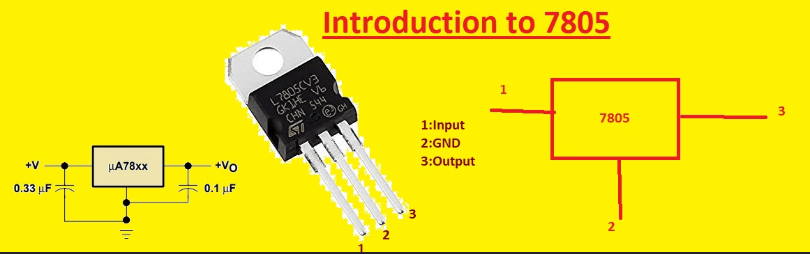
For linear fixed voltage regulators like the LM7805, the core of the polarization process lies in establishing a stable and reliable operating environment, rather than simply applying power. The critical aspect of this process is the proper use of decoupling capacitors at the input and output terminals. Regulators are highly sensitive to transient fluctuations in the power supply. Therefore, a polarized electrolytic capacitor (typically 10μF to 100μF) with correct polarity must be connected in parallel near the input pin, along with a non-polarized ceramic capacitor for high-frequency decoupling. The positive terminal of this electrolytic capacitor must be firmly connected to the positive terminal of the input voltage, while the negative terminal must be reliably grounded. The output terminal requires identical treatment: connect a polarized electrolytic capacitor with correct polarity to optimize load transient response. Reversing any capacitor polarity will cause rapid component heating and failure, preventing regulator startup. Additionally, ensuring the input voltage consistently exceeds the rated output voltage plus the “dropout voltage” is fundamental for proper operation. For example, the LM7805 requires at least 7V input to deliver a stable 5V output.
Polarization of Linear Voltage Regulators
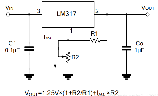
For linear adjustable voltage regulators like the LM317, polarity refers to actively setting its output voltage and establishing a reference point for operation. The core of this process involves configuring a precise resistive feedback network, which essentially provides the chip with the bias conditions necessary for proper functioning. You must connect a fixed resistor R1 (typically 240Ω) between the regulator's output pin and the adjustment pin (ADJ). This resistor establishes the minimum operating current required for the internal reference voltage within the chip. Subsequently, a second resistor R2 is connected between the adjustment pin and ground. Its resistance value directly determines the output voltage level, defined by the formula: Vout = 1.25V × (1 + R2 / R1). Connecting these two resistors constitutes the most critical polarizing operation for this chip; without them, the circuit will not function. Naturally, correctly connecting polarized capacitors at the input and output terminals to suppress ripple is equally indispensable for ensuring stable operation.
Polarization of Switching Voltage Regulators
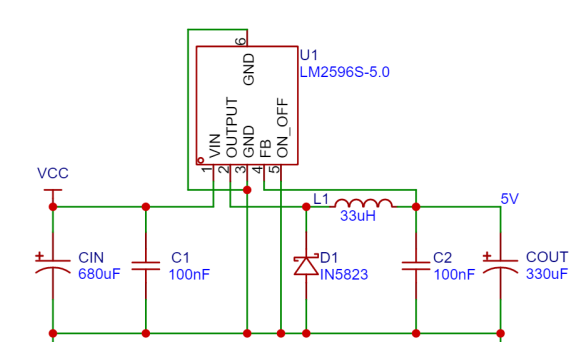
Switching voltage regulators (such as the LM2596) feature the most complex polarization, essentially requiring the construction of a complete switching power supply system around the chip. This process constitutes a systematic engineering endeavor involving the coordinated configuration and layout of multiple polarized components. First, a feedback network must be formed using two precision resistors. This network compares the sampled output voltage with the chip's internal reference voltage, dynamically controlling the switching duty cycle—the command center for voltage regulation. Second, the freewheeling diode in the power loop is a polarity-critical component. Its cathode must be firmly connected to the switch node (SW pin), while its anode must be grounded. Incorrect orientation in either direction causes a direct short circuit, instantly destroying the entire circuit. Finally, both input and output terminals require low-equivalent-series-resistance (ESR) electrolytic capacitors or tantalum capacitors with correct polarity to withstand massive switching ripple currents. Moreover, component placement on the PCB is critical: the loop area formed by the input capacitor, chip, and diode must be minimized to suppress switching noise—a “polarization” requirement at the PCB level.
The Universal Golden Rule for Polarized Voltage Regulators
1. Consult the Datasheet: This is the most critical step. Different models and brands of regulators may have specific requirements. The “Typical Application Circuit” section in the datasheet provides the official blueprint for polarity.
2. Verify Polarized Component Orientation: The direction of electrolytic capacitors, tantalum capacitors, and diodes is paramount in polarity operations. Double-check these components repeatedly. Before powering on, use the continuity setting on a multimeter to double-check for direct shorts.
3. Provide Correct Bias: Whether through a resistor network (e.g., LM317) or a feedback loop (e.g., switching regulator), supplying the chip with the bias conditions necessary for proper operation constitutes “polarization.”
4. Perform gradual power-up testing: For initial power-on, employ a “smoke test” (a humorous reference to preventing smoke) method: Use an adjustable current-limited power supply, initially set voltage and current limits low to observe if operating current is normal, then gradually increase to design values.
In summary, the “polarization” of voltage regulators is a component-specific, layered process. Its universal core lies in strictly adhering to the data sheet guidelines and ensuring the absolute correct orientation of all polarized components. For linear fixed regulators, polarization is fundamental, focusing on creating a stable operating environment through proper input and output capacitors. For linear adjustable regulators, polarization is configuration—the core lies in precisely commanding the desired output voltage through an external resistor network. For switching regulators, polarization is construction—a systematic engineering effort spanning feedback calculations, power component selection and placement, and PCB layout. Failure at any stage can lead to complete failure. Mastering these distinct approaches enables you to confidently start up and operate all types of voltage regulators safely and stably.
One-Stop HDI PCB Manufacturer and Its PCB Via Filing Capabilities
If you're looking for turnkey HDI electronics manufacturing services (EMS) from hardware development to PCBA fabrication and box-build assembly, you can work with the one-stop HDI PCBA manufacturer PCBONLINE.
Founded in 1999, PCBONLINE has R&D capabilities for HDI projects and EMS manufacturing capabilities, including via filling for stacked vias. It provides 4-to-64-layer HDI PCB fabrication, assembly, and PCBA box-build assembly. You can order various HDI PCBs from PCBONLINE, such as FR4, polyimide (flexible PCB), polyimide + FR4 (rigid-flex PCB), and PTFE/Rogers (high-frequency PCB).

3000m² of production capacity per day for HDI PCBs with builds of 1+N+1, 2+N+2, 3+N+3,4+N+4, and arbitrary interconnection in any layers.
PCBONLINE has hardware and software R&D capabilities for IoT applications requiring HDI design, including PCBA and enclosures.
We can manufacture complex PCBs with stacker vias, via-in-pad, microvias, inlay boards, heavy copper designs, and hybrid and fine structure lay-ups.
Besides HDI PCB fabrication, we have powerful capabilities in fine-pitch assembly for HDI PCB assembly.
We have rich R&D and manufacturing experience for HDI applications such as FPGA boards.
High-quality HDI PCB and PCBA manufacturing certified with ISO 9001:2015, IATF 16949, RoHS, REACH, UL, and IPC-A-610 Class 2/3.
Here'e the PCB via filing capabilities at PCBONLINEL:
- Micriavia filling with copper: laser via size 0.1-0.125mm, priority 0.1mm
- Finished hole size for via-in-pad filling with resin: 0.1-0.9mm (drill size 0.15-1.0mm), 0.3-0.55mm normal (drill size 0.4-0.65mm)
- Max aspect ratio for via-in-pad filling with resin PCB - 12: 1
- Min resin plugged PCB thickness: 0.2mm
- Max via-filling ith resin PCB thickness: 3.2mm
- Making different hole sizes with via filling in one board: Yes
- Via filling with copper/silver: Yes
If you need HDI PCBAs or any other PCBAs requiring via filling, please send your email to PCBONLINE at info@pcbonline.com. We will provide one-on-one engineering support to you.
Conclusion
Via filling is used for creating stacked vias in HDI PCB fabrication, BGA/CSP/QFN IC packaging, and filling PCB via-in-pad with resin during multilayer PCB fabrication. If you need one-stop electronics manufacturing for your HDI PCBA project, contact the one-stop advanced PCB manufacturer PCBONLINE for high-quality PCBA and box-build solutions tailored to your project's needs.
PCB fabrication at PCBONLINE.pdf


