
In Printed Circuit Boards (PCBs), electrical signals should be transmitted from one point to another without disruptions. In this article, we'll dive into PCB signal integrity, the common causes of signal degradation, and how you can tackle signal integrity challenges to create high-frequency PCBs!
In this article:
Part 1. What is PCB Signal Integrity and Why Does It Matter? Part 2. Challenges in Dealing with PCB Signal Integrity Part 3: Design-Related Causes of PCB Signal Integrity Issues Part 4. Best PCB Layout Practices for Signal Integrity One-stop High-speed and High-frequency PCB ManufacturerWhat is PCB Signal Integrity and Why Does It Matter?
PCB signal integrity refers to an electrical signal traveling from its source to its destination in a printed circuit board without noticeable distortion or noise. The signal integrity in PCBs is important because it measures the deterioration a signal experiences when moving through several components.
For lower frequencies, signal integrity might not be very important, but for high-speed signals like clock signals for high data rates, the significance of the impact of noise on an electrical signal increases. At higher frequencies, even minor distortions can significantly affect circuit performance.
Common manifestations of poor signal integrity include reduced noise margins, timing errors, distorted waveforms, and unintended noise coupling onto adjacent traces. Both analog and digital signals suffer from signal integrity issues while they move across the board.
Hence, PCB signal integrity also involves studying the analog behavior of high-speed digital signals during switching. Logic diagrams sometimes depict digital signals as tidy square waves, but their actual behavior is far rougher. These signals can become so corrupted at high rates that they are hardly identifiable as digital. This distortion occurs because the placement of components and routing of signals directly impacts signal behavior, especially in fast devices.
In short, if the placement of components and the routing of traces begin to significantly affect signal behavior, you're operating in a domain where signal integrity becomes critical.
For PCB designers, the consequences of inadequate signal integrity can be severe causing:
- Erroneous and unpredictable behavior of certain circuit components
- Complete malfunctioning of the PCB and associated systems
- Need for costly PCB redesigns and re-fabrication
Challenges in Dealing with PCB Signal Integrity
In PCB design, the challenges that cause PCB signal integrity problems are below.
1. Impedance mismatches
Impedance mismatches occur when the impedance of a signal trace does not match the connected components or transmission lines. This mismatch leads to signal reflections, which can distort the original signal and result in degraded performance.
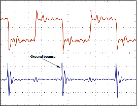
2. Ground bounce
Ground bounce is caused by the rapid switching of signals, which creates fluctuations in the ground voltage levels. This phenomenon is especially problematic in high-speed designs with densely packed vias and traces. This phenomenon is shown in the next image.
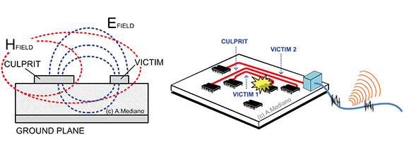
3. Crosstalk
Crosstalk occurs when electromagnetic fields from a signal trace induce interference in neighboring traces. The high density of traces or improper routing may cause crosstalk thus leading to data errors and signal degradation. The following image depicts the visualization of crosstalk in a PCB affecting one of the traces.
4. Electromagnetic interference (EMI)
High-speed signals are a common source of EMI if not managed correctly. Factors contributing to EMI include Trace Length and Configuration. These can also behave as antennas, amplifying EMI in the circuit and Signal Return Path.
Design-Related Causes of PCB Signal Integrity Issues
Beyond the specific phenomena listed above, certain design choices can exacerbate signal integrity problems:
Improper trace routing
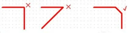
The PCB traces that contain sharp angles, or are highly twisted, the signal quality is severely reduced. To keep the signal as clean as possible, the trace should turn smoothly and gradually, avoiding sharp corners as depicted in the next image.
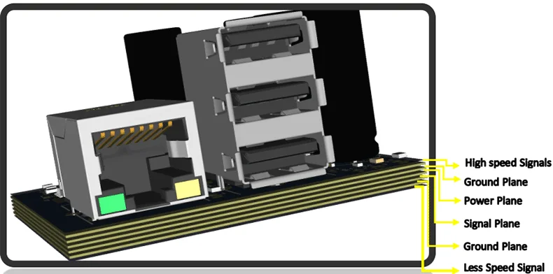
Layer stack mismanagement
Layer stack mismanagement refers to poorly designed or insufficient PCB layer configurations. The arrangement of signal layers, power planes, and ground planes is crucial for minimizing noise. Ideally, signal traces should be placed between two ground planes to act as a shield helping to reduce electromagnetic interference (EMI). A poorly designed layer stack can lead to unwanted effects like parasitic inductance or capacitance, which could disrupt the signals traveling through the board.
Inadequate decoupling capacitors
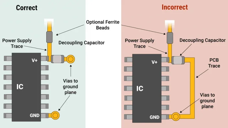
Decoupling capacitors help stabilize the power supply to prevent noise from disturbing the signals in sensitive circuits. However, if they're not properly chosen or placed, they can't do their job effectively. Therefore, these decoupling capacitors should be placed as close as possible to the power pins of active components and should have values that match the frequency characteristics of the circuit. The following image shows the routing recommendation for the decoupling capacitor.
To mitigate these issues, signal integrity analyses are performed. There are two basic kinds of signal integrity analysis:
(1) pre-layout design space exploration, which seeks to derive rules needed to place and route the board.
(2) post-layout verification, which seeks to simulate the PCB as designed to ensure it is reasonable to fabricate.
Best PCB Layout Practices for Signal Integrity
With an understanding of major signal integrity challenges, designers can utilize layout techniques to maintain signal quality in their PCBs. Here are some key signal integrity design guidelines.
Impedance matching
Impedance mismatch is a critical contributor to signal integrity. Setting the width and spacing of PCB traces according to the substrate material and layer structure is crucial for achieving proper impedance matching. For instance, in high-speed designs like USB 3.0 (90Ω differential impedance) or HDMI (100Ω differential impedance), controlled impedance traces are essential. Parameters such as trace width, spacing, dielectric constant, and the height from the reference plane must be carefully calculated.
Smart layer stack-up
Arrange layer stack-up to route sensitive traces over uninterrupted reference planes. Techniques like using microstrip (outer layer traces with a single reference plane) or stripline (inner layer traces between two reference planes) structures help maintain consistent impedance. Avoid routing signals over plane splits.
Leverage simulations
Pre-layout analysis explores stack-up arrangements and routing guidelines. Post-layout verification catches issues before fabrication. Advanced PCB design tools enable designers to implement many of these guidelines through features like constraint managers, real-time Design Rule Check, and crosstalk analysis.
One-stop High-Speed and High-Frequency PCB Manufacturer
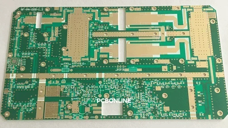
PCB signal integrity matters for high-speed and high-frequency PCBs, such as PTFE PCBs, Rogers PCBs, and HDI PCBs. For high-speed and high-frequency PCB one-stop manufacturing including R&D, you can work with the one-stop high-speed and high-frequency PCB manufacturer PCBONLINE, which provides R&D, PCB prototypes, PCB fabrication, component sourcing, PCB assembly for any high-speed and high-frequency projects without PCB signal integrity issues.

Founded in 1999, PCBONLINE has two large advanced PCB manufacturing bases, one PCB assembly factory, stable supply chains, and an R&D team.
Provide one-stop high-speed and high-frequency PCB manufacturing, including R&D, prototyping, PCB fabrication, component sourcing, PCB assembly, PCBA value-added, and box-build assembly.
Minimum laser drill: 0.075mm, minimum mechanical drill: 0.15mm, with microvia structures of 100 µm and 125 µm. High-density circuit layers up to 20, and microvia layers up to 64.
PCBONLINE grasps the core technologies for high-speed PCB manufacturing, such as impedance control, embedded antenna DFM, expansion/contraction control, etc.
Have ready-to-use high-speed PCB base materials in stock, and the storage period is within 45 days (at manufacturers who have no storage, it usually takes 2 to 3 months to purchase base materials).
High-quality high-speed and high-frequency PCB manufacturing certified with ISO 9001:2015, ISO 14001:2015, IATF 16949:2016, RoHS, REACH, UL, and IPC-A-600 Class 2/3.
PCBONLINE pays attention to quality and cost-effectiveness in high-speed and high-frequency PCBs. If you want to get a quote or ask questions about PCB signal integrity or your project, you can send emails to info@pcbonline.com.
Conclusion
PCB signal integrity ensures the seamless performance of the devices. High-speed signals are particularly susceptible to issues like impedance mismatches, ground bounce, crosstalk, and EMI, which can degrade the signal quality. However, employing the best practices like proper trace routing, impedance matching, and careful layer stack management can mitigate these effects. If you need high-speed and high-frequency PCBs, work with the one-stop PCBA manufacturer PCBONLINE.
PCB fabrication at PCBONLINE.pdf


