

In the era of IoT computing, GPU server, and high-speed network, Electromagnetic Compatibility (EMC) of the printed circuit board (PCB) is a baseline requirement.
For Radio Frequency (RF) designers, the PCB design challenge is preventing internal circuits from emitting interference and protecting sensitive components from external noise. We call it PCB shielding.
While the term PCB shielding might sound simple, the implementation involves a sophisticated mix of physics, material science, and strategic manufacturing.
PCBONLINE has rich experience in high-frequency PCB DFM (design for manufacturing) and manufacturing. In this guide, we explore the three primary methods of PCB shielding: Shielding Cans, Shielding Layers, and Via Stitching.
Understanding RF, EMI, EMC, and Other Shielding-Related Terms
Before diving into PCB shielding methods, we must define what EMI and EMC are, and what RF means.
EMI (Electromagnetic interference): The actual disturbance caused by electromagnetic radiation. In RF PCBs, this is often "crosstalk" between high-frequency traces or radiation from an antenna affecting a local power regulator.
EMC (Electromagnetic compatibility): The ability of a device to function in its environment without causing or suffering from EMI.
RF shielding: The physical practice of using conductive materials to create a Faraday Cage around specific circuits, effectively blocking electric fields.
![]()
Besides RF, EMI, and EMC, the PCB shielding-related terms are below.
- Skin effect: At high frequencies, current tends to flow on the surface of a conductor rather than through its center. This is why the surface finish and material of a shield are critical for performance.
- Crosstalk: The unwanted transfer of energy between two parallel traces. Shielding (like via stitching or guard traces) is the primary cure for crosstalk.
- Shielding frame & lid (two-piece shield): Consists of a "fence" soldered to the PCB and a removable cover. It is the gold standard for testability.
- Shielding clips: Small, surface-mount spring clips that hold a metal shield in place without soldering the shield itself. This allows for easy removal during repair.
- Conductive elastomers: Rubber-like gaskets loaded with silver or nickel particles. These provide both EMI shielding and a moisture seal.
- Fingerstock: Conductive strips made of beryllium copper with "fingers" that provide a flexible, high-conductivity seal between a PCB and a metal enclosure.
- Guard ring: A grounded copper trace that surrounds a sensitive analog signal or a noisy high-speed signal to catch any lateral interference.
Having understood these PCB sheilding related terms, now let's explore the three PCB shielding methods and their DFM.
Shielding Cans (The Physical Barrier)
The metal Shielding Can is the most robust form of localized protection for PCB shielding.
It is a conductive enclosure placed directly over specific components, such as a Bluetooth module, a cellular transceiver, or an FPGA.
How does a shielding can work?
A shielding can create a grounded conductive box. When an electromagnetic wave hits the metal surface, it induces currents within the conductor, which are then shunted to the ground plane, preventing the wave from penetrating the enclosure.
DFM for Shielding Cans
PCB shielding using a metal involves not only its size but also how it interacts with the assembly SMT line. At PCBONLINE, our DFM checks —
- Solder trace width: The "fence" (the footprint where the can sits) must have sufficient width (typically 1mm to 2mm) to ensure a strong mechanical bond.
- Thermal relief: Because the shield acts as a massive heat sink, you must use thermal reliefs on ground connections to prevent "cold solder joints" during reflow.
- Height clearance: Ensure the can's ceiling is at least 0.2mm - 0.5mm higher than the tallest component it covers to avoid short circuits.
- Testability: A major DFM pitfall is the "Blind Spot." Permanent surface-mount cans prevent AOI (Automated Optical Inspection) and X-ray inspection of the components underneath. To solve this, our experts recommend Two-Piece Shielding or Clip-on Shields, allowing the lid to be snapped on after inspection.
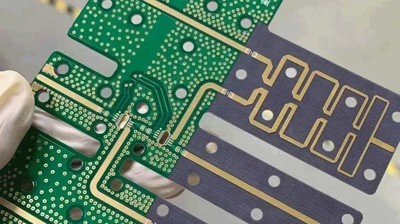
Shielding Layers (The Internal Fortress)
In multilayer PCBs, the internal stackup is your first line of defense.
Its implementation involves dedicated copper layers (usually Layer 2 and Layer n-1) that act as a continuous shield for internal signal traces.
- Stackup symmetry: To prevent board warping during the high-heat reflow process, the copper distribution in the stackup must be symmetrical.
- Copper poured density: Ensure consistent copper density across the layer to maintain uniform impedance control for RF traces.
- Proximity to signal layers: The closer the ground shield is to the signal layer, the better the EMI containment, but this requires precise prepreg thickness control during lamination.
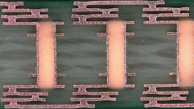
Via Stitching (The Electromagnetic Wall)
Via stitching involves placing a row of grounded vias along the perimeter of the PCB or along a specific high-speed trace to create a "picket fence" shield.
How does via stitching work for PCB shielding?
If the spacing between the vias is significantly smaller than the wavelength (λ) of the frequency being shielded (typically Pitch < λ/20), the electromagnetic wave "sees" the row of vias as a solid wall.
DFM for Via Stitching
- Via pitch vs. drill size: Vias placed too close together can weaken the structural integrity of the PCB substrate (the postage stamp effect).
- Solder mask tenting: Ensure vias are tented or filled if they are near SMT pads to prevent solder "wicking" away from the component pads into the via holes.
- Ring size: Maintain a minimum annular ring to ensure the vias remain connected to the ground planes even with slight manufacturing drill offsets.
PCB Shielding Case Study
At PCBONLINE, our expertise goes beyond PCB fabrication and assembly. We focus on Front-End Loading, where our DFM engineers identify risks before a single cent is spent on materials.
A recent project involving PCB shielding is a Shared Scooter IoT Mainboard, which highlights how professional DFM saves both time and money.
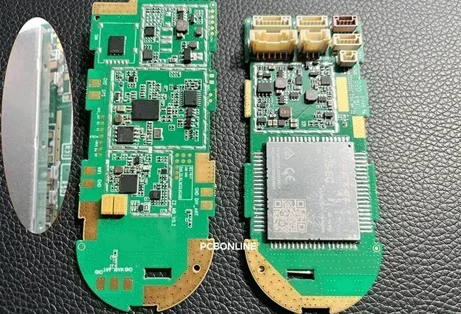
The background: A client approached us with a finished design for an IoT mainboard. They hadn't consulted us during the R&D phase, and the design had several latent risks regarding testing and cost.
The PCBONLINE DFM Solution
Our engineers performed a rigorous "Production-Ready" check and implemented three critical changes:
- 1. Solving the inspection paradox
The client's original design used Fixed Surface-Mount Shielding Cans.
The issue is that, once soldered, components under the can (like the critical communication module) could not undergo AOI or X-RAY inspection. Any soldering defect would remain hidden until the final functional test, leading to expensive rework.
We suggested switching to Snap-on/Clip-style Shielding Cans. This allowed our team to perform full AOI and X-ray inspections on the SMT components first, then snap the lids on. The client agreed, drastically improving the yield rate.
- 2. Footprint vs. BOM reconciliation
During the DFM process, we discovered that three passive component models in the BOM (Bill of Materials) had specifications that didn't match the PCB land patterns (pads).
The risk is that, without this catch, the assembly line would have stopped mid-run because the components wouldn't fit the pads.
We alerted the client immediately, allowing them to adjust the PCB traces and pads before production, avoiding a total project stall.
- 3. Strategic sourcing for IoT modules
Because PCBONLINE maintains strategic partnerships with original chip manufacturers and Tier-1 agents, we have immense bargaining power, especially for IoT Communication Modules.
By leveraging our centralized procurement, we helped the client save 15% on total component procurement costs, and at least 10% on general passive components.
Partner with PCBONLINE for Turnkey RF PCBs
After you complete the EMI shielding validation, does it ensure the successful manufacturing of your project? Not yet. You will need a high-frequency PCB manufacturer, PCBONLINE, with rich DFM (design for manufacturing) experience to ensure no technical and non-technical issues for a seamless manufacturing process.

Founded in 1999, PCBONLINE has two large advanced PCB manufacturing bases, one PCB assembly factory, and an R&D team. For high-frequency PCB manufacturing, PCBONLINE is equipped with a plasma cleaning machine, laser drilling equipment, thermal shock equipment, and an accurate etching line.
PCBONLINE provides free professional DFM before and during fabrication for your entire project, including PCB EMI shielding, and can offer improvement suggestions.
Complete high-frequency PCB manufacturing and testing, including mature etching technology, plasma treatment, trace width compensation with ±0.015mm accuracy, strict solder mask thickness control, and thermal shock at 288℃ for 10 seconds, 1 to 3 times.
PCBONLINE has in-stock high-frequency laminates to reduce the PCB manufacturing lead time. Besides, for the best quality and performance of the PCB, our laminate storage time is within 45 days.
High-frequency PCBs made of any type of material and laminate brands are accessible, such as embedded antenna PCBs, PTFE, ceramic, PTFE/ceramic hybrid, Rogers, Taizhou Wangling, Taconic, etc.
No MOQ, and no matter what quantity you want, we prioritize quality. The high-frequency PCBs and PCBAs are certified with SO 9001:2015, ISO14001:2015, IATF 16969, RoHS, REACH, UL, IPC-A-600 Class 2/3, and IPC-A-610 Class 2/3.
Conclusion
Effective RF PCB shielding requires a holistic approach. While Shielding Cans provide the best isolation, Layer Shielding and Via Stitching provide the necessary internal architecture. However, as shown by the PCBONLINE IoT case study, the best technical design can still fail if it doesn't account for inspectability and component availability. If you are looking for a trusted partner for RF PCBs, contact PCBONLINE for turnkey OEM manufacturing with our PCB shielding DFM.
PCB assembly at PCBONLINE.pdf


