
In the fast-paced world of electronics, PCB reverse engineering is a sophisticated process used to understand, replicate, or improve upon an existing circuit board.
Whether you are looking to repair a vintage piece of equipment that no longer has manufacturer support or you want to analyze a competitor's design, reverse engineering is a powerful tool.
However, the practice sits at a crossroads of technical brilliance and legal complexity.
What is PCB Reverse Engineering?
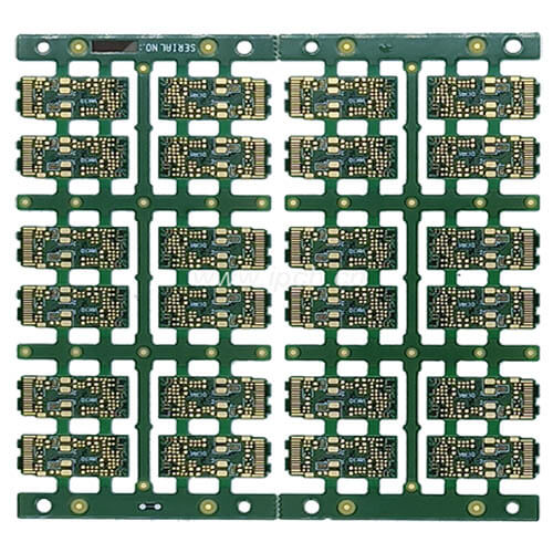
PCB reverse engineering is the process of analyzing a physical printed circuit board to recreate its schematics, Bill of Materials (BOM), and Gerber files.
Instead of starting with a design and building a board, you start with the printed circuit board and work backward to the design files.
Why Reverse Engineer a PCB?

- Obsolete technology: Recreating boards for machines where the original manufacturer has gone out of business.
- Cost reduction: Identifying expensive components in a design that could be replaced with modern, cheaper alternatives.
- Security auditing: Checking a board for "hardware backdoors" or unintended vulnerabilities.
- Competitive analysis: Understanding the technical benchmarks of a competitor's product.
How to Copy a PCB Board: A Step-by-Step Guide
Copying a PCB is a meticulous process that requires patience and the right tools. Here is the standard workflow:
- 1. Preparation and Cleaning
Before starting, the PCB must be cleaned of all dust and debris. Take high-resolution photographs of both sides of the PCB. These photos serve as a primary reference point to ensure components are placed correctly during the "forward" engineering phase. - 2. Component Removal (Destructive vs. Non-Destructive)
To see the traces hidden under components, you often need to desolder them.
Non-destructive: Carefully desoldering components to preserve them.
Destructive: Grinding down layers of a multi-layer board to see internal traces (used for complex 4+ layer boards). - 3. Scanning and Imaging
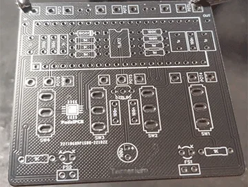
The bare PCB is placed on a high-resolution industrial scanner. This creates a 1:1 scale image of the copper traces. For multi-layer boards, this process is repeated for every layer. - 4. Trace Routing and Schematic Capture
Using CAD software (like Altium, Eagle, or KiCad), the scanned images are used as a "template." Engineers draw lines over the scanned traces to recreate the digital layout. This allows the software to generate a netlist, which identifies how every component is connected. - 5. Recreating the Schematic
Once the traces are mapped, the engineer creates a readable circuit schematic. This is the "brain" of the circuit board, showing the logical flow of electricity and data.
Is It Legal to Copy a PCB?

The legality of PCB reverse engineering is not a simple "yes" or "no." It depends heavily on intent and jurisdiction.
When It Is Generally Legal:
- Repair and Maintenance: If a manufacturer no longer supports a product, reverse engineering for the sake of repair is often protected under "Right to Repair" concepts.
- Interoperability: In many regions, you can reverse engineer a product to ensure your own product can work with it (e.g., creating a third-party charging cable).
- Education and Research: Analyzing a board to understand how it works for academic purposes is typically considered "Fair Use."
When It Is Illegal:
- Patent Infringement: Even if you redraw the circuit board from scratch, if the circuit design itself is patented, you cannot legally manufacture or sell it.
- Copyright Violation: The "artwork" of the PCB (the specific layout of the traces) can be protected by copyright. Direct 1:1 copying for commercial gain is a high-risk area.
- Trade Secrets: If you obtained the circuit board through a non-disclosure agreement (NDA) or theft, reverse engineering it is a violation of trade secret laws.
If you plan to sell a product based on reverse engineering, always consult with an Intellectual Property (IP) attorney to ensure your "new" design is sufficiently transformative.
Partner with PCBONLINE for Quick-Turn PCBs
If you need B2B one-stop, quick-turn PCB manufacturing and assembly, you can partner with PCBONLINE. By separating their services into Express (8 Hours) and Technical Quick-Turn (3-5 Days), we provide a tailored solution for every stage of the product lifecycle.
Founded in 2005, PCBONLINE has two large advanced PCB manufacturing bases, one PCB assembly factory, stable supply chains, and an R&D team for one-stop PCBA manufacturing.
PCBONLINE has strong PCB manufacturing capabilities, including FR4 PCB layers from 1 to 64, thick-copper PCB up to 14oz, high-frequency PCBs, flexible PCB, rigid-flex PCB, aluminum PCB, copper-based PCB, and ceramic PCB.
PCBONLINE offers free design for manufacturing (DFM) for your PCB and PCBA project, including checking Gerber, bill of materials (BOM), testing files, and solving all technical and unexpected issues during prototyping to ensure the smooth and successful massive production.
Speed: 8 working hours for standard FR4, Aluminum, and 1-layer FPC.
Stock: A warehouse with over 1 million components to facilitate 8-hour assembly.
Global Logistics: Reliable air shipping to the US in 2-3 days from the Shenzhen hub.
High-quality advanced PCB manufacturing certified with ISO 9001:2015, ISO 14001:2015, IATF 16949:2016, RoHS, REACH, UL, and IPC-A-600 Class 2/3.
No matter what power applications of your PCB are, like automotive, aerospace, medical devices, industrial controls, and mid- to high-end consumer electronics, PCBONLINE can produce and assemble PCBs that meet the highest performance and reliability standards. To get a quote for your B2B quick-turn PCB, contact info@pcbonline.com.
Conclusion
PCB reverse engineering is an essential skill for hardware recovery and innovation. While the technical process involves high-res scanning and CAD routing, the legal side requires a deep understanding of patents and copyrights. When done ethically and legally, it bridges the gap between old hardware and future possibilities.
PCB assembly at PCBONLINE.pdf
PCB fabrication at PCBONLINE.pdf


