
PCB assembly can be divided into three stages: preparation stage, assembly stage, and post-stage. This blog will also introduce the process of these three stages in detail.
In this article:
Part 1. Required documents and designs Part 2. The PCB Assembly Process Stage Part 3. After PCB assemblyRequired Documents and Designs
Design files usually include schematics, PCB layouts, Gerber files, BOMs, 3D models, etc. The design points to pay attention to include signal integrity, EMC, thermal management, DFM, etc. Engineers hand over the design to manufacturers, so they need to ensure the correctness of the files to avoid production errors.
Usually, a complete design file includes the following:
Schematic
Format: .sch (Altium Designer), .dsn (Cadence) or PDF document.
PCB Layout
Format: .pcb (Altium), .brd (Cadence Allegro), etc.
Gerber file
Including files:
Top/bottom copper layer (.GTL, .GBL)
Silk screen layer (.GTO, .GBO)
Solder mask layer (.GTS, .GBS)
Drill file (.DRL or .TXT)
(BOM)
Content: component model, package, quantity, supplier, reference number, etc.
Format: Excel table or CSV file.
Sometimes, according to customer needs, 3D model files, design rule check reports and function test reports are also provided.
The manufacturer's R&D team will check the design documents one by one, such as whether there are replaceable models for the component specifications on the BOM, whether there are open circuit problems in the layout, whether the design of the top and bottom layers of the PCB is reasonable, etc.
The PCB Assembly Process Stage
In fact, PCBA refers to Printed Circuit Board Assembly, which is an assembled circuit board, while PCB is a bare board. However, some people may think that the two are the same process. It is necessary to distinguish the two concepts here. The detailed process described below belongs to PCBA
Solder Paste Printing
First, the bare PCB is fixed on the workbench of the printer, and the Stencil is precisely aligned with the surface of the PCB. The surface of the Stencil has holes corresponding to the positions of the pads on the PCB. These holes determine the position and shape of the solder paste printing. Therefore, each stencil needs to be specially customized. The Squeegee moves on the stencil, scraping the solder paste evenly into the holes of the stencil and then transferring it to the pads of the PCB through the holes. The stencil is lifted, and the solder paste printing is completed. At this point, the appropriate amount of solder paste has been accurately printed on the pads of the PCB.
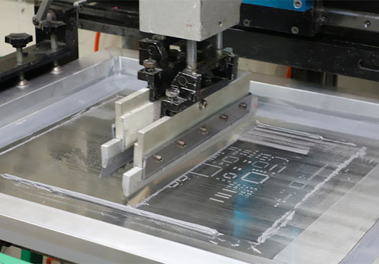
After completion, there will be a process called Solder Paste Inspection (SPI), which is mainly used to detect the accuracy and consistency of solder paste printing to ensure the reliability of subsequent reflow soldering.
At this step, if the PCB is assembled with BGA components, X-Ray inspection is required after completing SPI. The details of X-ray inspection are described below.
X-Ray inspection(optional, used for special packaging components such as BGA)
For some unique packaged components, such as BGA (Ball Grid Array), visual inspection and AOI cannot detect the internal soldering quality because the solder joints are packaged at the bottom of the component. X-ray inspection can penetrate the component through X-rays and image the condition of the solder joints inside the element, thereby detecting defects such as cold solder joints and voids in components such as BGA.
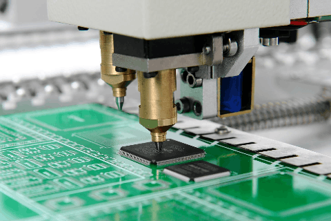
Component Placement
Prepare the required SMD components first. These components are usually fed to the placement machine in the form of tape, tray or tube.
The placement machine needs to be pre-programmed to import the component coordinate information and component library of the PCB in order to identify the component type and placement position.
The nozzle of the placement machine picks up the components from the feeder.
However, some high-end placement machines have a visual recognition system that can identify the model and direction of the component to ensure the accuracy of the placement.
The placement machine accurately places the components on the pads on the PCB where the solder paste has been printed according to the coordinates set by the program (X, Y, Z axis). The viscosity of the solder paste can temporarily fix the components to prevent them from shifting during the movement.
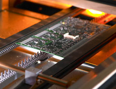
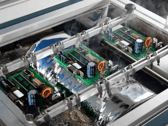
Reflow Soldering
The PCB with mounted components is conveyed to the reflow oven.
When the PCB enters the preheating area, the temperature gradually rises, the flux in the solder paste begins to activate, and the oxides on the pads and component surfaces are removed. At the same time, preheating can reduce the thermal shock of the PCB and components in the subsequent high-temperature stage and prevent breakage caused by sudden heat.
After that, the PCB gets to the constant temperature area, where the temperature remains relatively stable, making the temperature of the PCB and components tend to be uniform, further activating the flux and reducing the generation of air bubbles.
Then, the PCB gets to the reflow area, where the temperature rises rapidly above the melting point of the solder paste, the solder paste begins to melt, and the liquid solder wets the pads and component pins to form solder joints. The peak temperature and time need to be strictly controlled to ensure that the solder is fully melted while avoiding overheating damage to the components and PCB.
AOI Testing
Use AOI equipment to automatically scan PCB components and automatically detect soldering defects and mounting defects through image analysis technology.
AOI inspection can improve inspection efficiency and accuracy and reduce omissions in manual inspection.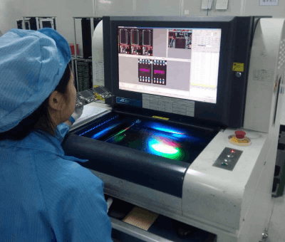
Wave Soldering(Optional step, usually for through-hole components)
This step involves manual labor, and through-hole components need to be manually inserted into the holes of the PCB.
A layer of flux is then applied to the bottom of the PCB to remove oxides and improve soldering quality.
The PCB gets to the preheating zone, which increases the temperature of the PCB and activates the flux.
A wave of liquid solder passes through the bottom of the PCB, and the liquid solder wets the pins of the through-hole components and the PCB pads to achieve soldering.
After soldering is completed, the PCB enters the cooling zone, and the solder joints solidify.
After PCB assembly
After the PCB is assembled, there are several important inspection processes, including software and hardware.
Functional Testing
According to the function of PCBA, the test plan is designed, the test program is written, the test platform is built, and the PCBA is fully functionally tested.
The test content includes:
Electrical performance test: a series of voltage, current, power, signal transmission and other parameter tests are carried out.
Functional module test: for example, each functional module of PCBA is tested, such as the above single chip microcomputer/IC, etc., to verify whether its function is normal.
Reliability test: In some cases, high temperature, low temperature, vibration and other environmental tests are also required to verify the reliability of the working environment of PCBA.
Cleaning
Use ultrasonic cleaning, water-based cleaning, solvent cleaning and other methods to remove residual flux and other contaminants on the PCBA surface to improve the cleanliness and reliability of PCB components.
Coating
To improve the reliability of PCBA in harsh environments, such as humid, corrosive, dusty, etc., a protective coating can be applied to the surface of PCBA, such as three-proof paint (moisture-proof, mildew-proof, and salt spray-proof). Manufacturers usually use brushing, dipping, spraying and other methods for coating.
Final Inspection and Packaging
Manually check whether the PCBA's appearance and functions are normal. Use anti-static bags, foam and other materials to protect the PCBA to prevent damage during transportation.
In short, although each manufacturer’s specific production processes and equipment used may be different, in general, most manufacturers can hardly avoid each of the processes mentioned above.
One-Stop HDI PCB Manufacturer and Its PCB Via Filing Capabilities
If you're looking for turnkey HDI electronics manufacturing services (EMS) from hardware development to PCBA fabrication and box-build assembly, you can work with the one-stop HDI PCBA manufacturer PCBONLINE.
Founded in 1999, PCBONLINE has R&D capabilities for HDI projects and EMS manufacturing capabilities, including via filling for stacked vias. It provides 4-to-64-layer HDI PCB fabrication, assembly, and PCBA box-build assembly. You can order various HDI PCBs from PCBONLINE, such as FR4, polyimide (flexible PCB), polyimide + FR4 (rigid-flex PCB), and PTFE/Rogers (high-frequency PCB).

3000m² of production capacity per day for HDI PCBs with builds of 1+N+1, 2+N+2, 3+N+3,4+N+4, and arbitrary interconnection in any layers.
PCBONLINE has hardware and software R&D capabilities for IoT applications requiring HDI design, including PCBA and enclosures.
We can manufacture complex PCBs with stacker vias, via-in-pad, microvias, inlay boards, heavy copper designs, and hybrid and fine structure lay-ups.
Besides HDI PCB fabrication, we have powerful capabilities in fine-pitch assembly for HDI PCB assembly.
We have rich R&D and manufacturing experience for HDI applications such as FPGA boards.
High-quality HDI PCB and PCBA manufacturing certified with ISO 9001:2015, IATF 16949, RoHS, REACH, UL, and IPC-A-610 Class 2/3.
Here'e the PCB via filing capabilities at PCBONLINEL:
- Micriavia filling with copper: laser via size 0.1-0.125mm, priority 0.1mm
- Finished hole size for via-in-pad filling with resin: 0.1-0.9mm (drill size 0.15-1.0mm), 0.3-0.55mm normal (drill size 0.4-0.65mm)
- Max aspect ratio for via-in-pad filling with resin PCB - 12: 1
- Min resin plugged PCB thickness: 0.2mm
- Max via-filling ith resin PCB thickness: 3.2mm
- Making different hole sizes with via filling in one board: Yes
- Via filling with copper/silver: Yes
If you need HDI PCBAs or any other PCBAs requiring via filling, please send your email to PCBONLINE at info@pcbonline.com. We will provide one-on-one engineering support to you.
Conclusion
Via filling is used for creating stacked vias in HDI PCB fabrication, BGA/CSP/QFN IC packaging, and filling PCB via-in-pad with resin during multilayer PCB fabrication. If you need one-stop electronics manufacturing for your HDI PCBA project, contact the one-stop advanced PCB manufacturer PCBONLINE for high-quality PCBA and box-build solutions tailored to your project's needs.
PCB fabrication at PCBONLINE.pdf


