
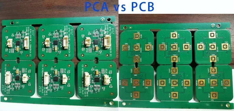
In electronics design and manufacturing, the two terms PCB and PCA are commonly seen. They refer to distinct stages of printed circuit boards. PCBONLINE, an OEM PCB manufacturer for terminal companies’ engineers, project managers, and purchasing teams, provides one-stop printed circuit board manufacturing and assembly.
Our article provides a comparison of PCA vs PCB and explains how a bare PCB becomes a functional assembly.
What are PCB and PCA
Before diving into the differences between PCB and PCA, let’s learn about what they are, respectively.
PCB: Printed Circuit Board
A printed circuit board (PCB) is an unpopulated circuit board with no electronic components mounted. It provides electrical interconnection with copper traces, vias, and PCB pads, and offers mechanical support and thermal dissipation for electronic components.
In Japan and some aerospace/military contexts, PWB (printed wiring board) is used as an alternative term for PCB.
A PCB consists of a base or core and layers of non-conductive dielectric material laminated with copper foil. Common base materials include:
- FR4: Glass-fiber epoxy, used in most consumer and industrial products
- Polyimide (PI): Flexible and lightweight, used for flexible or compact products
- PTFE (Teflon): Extremely low Dk/Df for RF, microwave, and 5G applications
- Metal-core (aluminum, copper): For high-power LED and power conversion modules
- Ceramic (Al₂O₃, AlN): For high-reliability, high-thermal-conductivity electronics
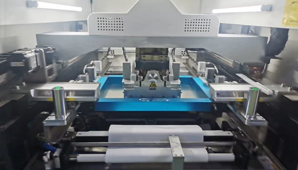
PCB fabrication process involves multiple manufacturing steps:
- Lamination – bonding layers of prepreg, core, and copper
- Drilling – mechanical or laser drilling of vias and holes
- Copper plating – creating via interconnections through electroless/electrolytic plating
- Imaging & etching – forming the circuit pattern
- Solder mask coating – insulating and protecting traces
- Surface finish – ENIG, HASL, OSP, immersion silver, etc.
- Electrical testing – verifying connectivity to the designed netlist
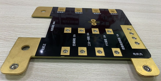
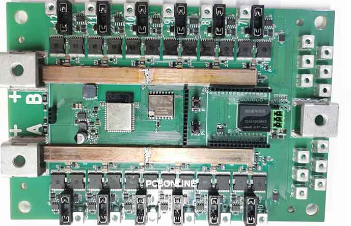
PCA: Printed Circuit Assembly, or PCBA
PCA is a printed circuit assembly (PCA) and is more commonly called PCBA. It is a fully assembled and functional circuit board, mounted with all required components.
A PCA is a functional electronic board that performs power conversion, RF communication, signal processing, sensing, or computing. Unlike the bare PCB, it contains all active and passive components required by the schematic.
Depending on the complexity of the final product, a PCA may serve as:
- A complete product, such as smart IoT environmental sensor boards
- A subsystem, such as motherboards, daughterboards, and power boards
- A functional module, such as Wi-Fi modules and motor driver modules
- One of multiple coordinated PCAs forming a complete system
During and after the circuit board assembly process, a PCA is tested, validated, and integrated into an enclosure or system.
PCA is often a semi-product inside a larger system, or it may serve as a standalone module, such as a Wi-Fi/LoRa/BLE communication module, power supply module, Microcontroller processor board, sensor board, or motor control board.
A PCA becomes functional through solder joints that electrically connect components to the PCB pads. These solder joints form the critical metallurgical interface that determines mechanical strength and reliability.
Printed Circuit Assembly Process
The process to turn a PCB into a PCA is known as PCB assembly. PCA manufacturing involves Surface Mount Technology (SMT) and Through-Hole Technology (THT).
SMT: Automatic Mounting SMDs on PCB Surface
The SMT workflow transforms a blank PCB into a functional electronic assembly or module. It is processed by:
Step 1. Solder paste printing and inspection
A stainless steel stencil deposits solder paste onto copper pads. Paste quality and alignment accuracy are essential for:
- Fine-pitch QFN and QFP devices
- Micro BGAs and CSP packages
- 0201/01005 miniature passives
After solder paste printing, a solder paste inspection machine scans the solder paste on PCB pads to ensure its solderability.
Step 2. SMD placement
Pick-and-Place machines position components according to:
- BOM (Bill of Materials)
- Centroid placement file
- CAD/ODB++ data
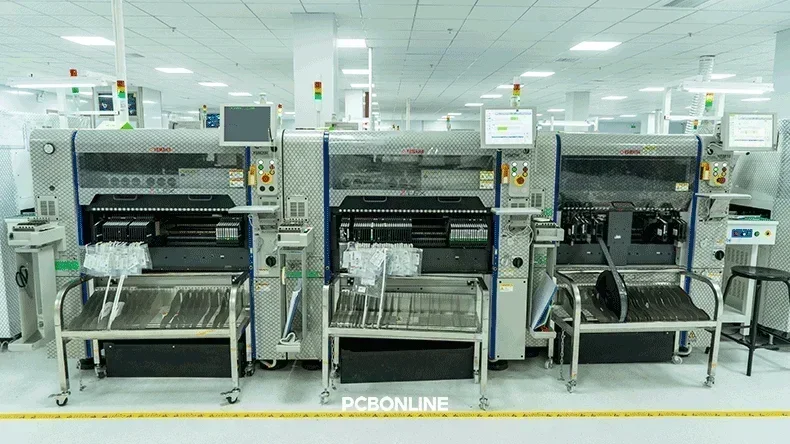
At PCBONLINE, each of our four SMT lines is equipped with two YAMAHA YSM20R machines and one YSM10 machine for SMD placement, supporting up to 376 components per PCB, with positional accuracy down to micrometers.
Step 3. Pre-reflow AOI
At PCBONLINE, each of our SMT lines is equipped with dual AOI (automated optical inspection) systems, one before reflow soldering, the other following reflow.
After SMD placement, the PCB passes our pre-reflow AOI machine, where it is scanned and analyzed to ensure no soldering risks, such as component missing or excess, potential of poor soldering, component position offset, etc.
Our pre-reflow AOI prevents economic losses due to a defective reflow soldering process.
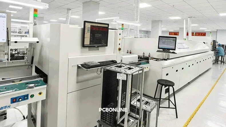
Step 4. Reflow soldering
The PCB passes through a multi-zone reflow oven. The temperature profile is engineered to:
- Activate flux
- Melt solder
- Form intermetallic bond layers
- Minimize voids and thermal shock
Our engineers have rich experience in oven temperature control, which is essential for BGA, LGA, and CSP packages.
Step 5. AOI and optional X-ray inspection
Our pro-reflow AOI checks for tombstoning, insufficient solder, shorts, and opens.
If your PCB contains hidden-joint components, like BGA, QFN with thermal pads, or bottom-terminated components, we have an X-ray inspection to ensure its hidden joints create a good connection.
THT: Half-automated Through-Hole Soldering
Although SMT dominates electronics manufacturing, THT remains essential for high-current connectors, transformers and inductors, relays, large electrolytic capacitors, and mechanical interfaces requiring robustness.
THT soldering is done by inserting leads of through-hole components through the PCB holes and using wave soldering or selective soldering. After wave soldering, we trim the leads to 1-2mm and clean the PCAs.
If our client requires value-added services to the PCA, we can also have a functional test, conformal coating, IC programming, and burn-in test. At last, we install the PCA into the enclosure and make it a finished device.
PCB vs PCA
The difference between PCB and PCA determines who handles what part of the production, how much each step costs, and how quality is controlled.
|
|
PCB
|
PCA
|
|
Manufacturing stage
|
Fabrication
|
Assembly (SMT/THT)
|
|
Functionality
|
Non-functional
|
Fully functional
|
|
Primary cost drivers
|
Material, stack-up, vias, copper weight, line/space
|
BOM cost, component sourcing, SMT/THT complexity, testing
|
|
Quality standard
|
IPC-6012
|
IPC-A-610
|
|
Testing required
|
Electrical continuity (E-test)
|
ICT, FCT, AOI, X-ray, burn-in
|
Partner with PCBONLINE for OEM PCB and PCA
Since the foundation in 2005, PCBONLINE has been committed to turnkey OEM PCB and PCA. We focus on PCBA manufacturing from prototypes to mass production. We can also provide box-build assembly to the PCA, a module, and the final device.
Our turnkey OEM PCBA services offer:
- Turnkey PCBA manufacturing: From PCB ptototypes and testing to mass PCBA and box-build assembly, our PCB assembly services are custom and one-stop.
- Complete procurement: We source and customize enclosures, cables, and accessories from reliable suppliers.
- Engineering support: We check enclosure and accessory designs for compatibility with your PCBA and can suggest design changes.
- Free DFM/DFT: We provide free Design for Manufacturability (DFM) and Design for Testability (DFT) checks to ensure that designs are optimized for a smooth production process.
- Quality assurance: IPC-A-610 Class 2/3, automotive-grade or industrial-grade inspection standards.
- Turnkey delivery: From PCB fabrication to final product packaging and shipping.
PCBONLINE manufactures, assembles, and tests PCBs and PCBAs to box builds as a source factory manufacturer under one roof, from prototypes to bulky production, saving costs and time for you.
We have powerful manufacturing strength for advanced PCBs and high-end assemblies, such as HDI PCBs, high-frequency PCBs, ceramic PCBs, waterproof sealing, and 01005 fine-pitch assembly.
We can precisely control reflow/wave oven temperatures, design PCBA fixtures, and help create user manuals, installation guides, and compliance labels.
Our high-quality PCBA contract manufacturing is certified with ISO 9001:2015, ISO 14001:2015, IATF 16949:2016, RoHS, REACH, UL, and IPC-A-610 Class 2/3.
Our one-on-one free and professional DFM helps you debug and improve design, to ensure the manufacturability, cost-effectiveness, and final device success.
Whether you need turnkey OEM PCB manufacturing and assembly for server automatic transfer switches, AI hardware, IoT devices, medical-grade products, or automotive modules, we can deliver the PCBAs and modules of high quality and in time, meeting any of your project requirements. To get a quote for your PCBA or custom module project, email us at info@pcbonline.com.
Conclusion
PCB is the bare foundation of electronic products to support and connect components, defined by materials, stack-up, copper geometry, and fabrication tolerances. PCA is a fully assembled and functional board or module, defined by assembly quality, solder joint integrity, testing, and value-added services. PCBONLINE is a reliable OEM PCB and PCA manufacturer providing one-on-one engineering support and turnkey electronics manufacturing. If you want to order or consult about PCBs or PCAs, don't hesitate to contact PCBONLINE.
PCB fabrication at PCBONLINE.pdf
PCB assembly at PCBONLINE.pdf


