
What is a PCB pad? Is it different from a PCB via? You can get a clear insight into what a PCB pad is in this post by the OEM PCB manufacturer PCBONLINE.
What is a PCB Pad
A PCB pad is also called a PCB contact, which is a small surface of copper in a printed circuit board that permits binding the component to the board. You can consider a pad a piece of copper where the pins of the part are precisely upheld and bound.
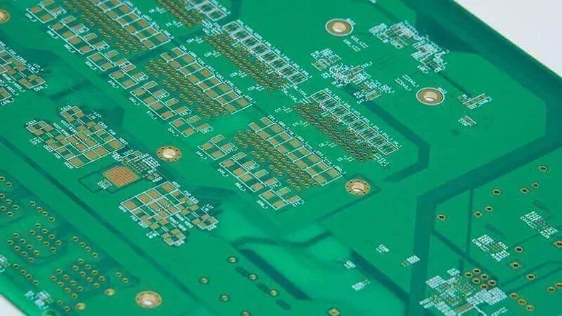
There are 2 sorts of pads: through opening and SMD (surface mount).
- Through the opening pad
Through-opening pads are expected for presenting the pins of the parts, so they can be welded from the contrary side from which the segment was embedded. These sorts of pads are fundamentally the same as a through opening by means of.
- SMD pad
The SMD pads are expected for surface mount devices, or all in all, for welding the segment on a similar surface where it was put.
Surface Land PADs
Surface land pads are the zones on the PCB to which the solder balls follow. The size of these pads influences the space accessible for vias and for avoiding steering. Generally, surface land pads are accessible in the accompanying two essential plans:
- Non-solder mask defined (NSMD)
- Solder mask defined (SMD)
The fundamental contrasts between the two surface land pad types are the size of the follow and the separation between the follow lines, the kind of vias you can utilize, and the state of the solder balls after solder reflow.
- Non-Solder Mask Defined
In the NSMD pad, the solder mask opening is bigger than the copper pad. Hence, the surface land pad's copper surface is totally uncovered, giving more noteworthy region for which the solder ball can follow. Allude to Figure 2 for the Side View of NSMD and SMD Land Pads.
- Solder Mask Defined
In an SMD pad, the solder mask covers the surface land pad's copper surface. This cover gives more prominent bond strength between the copper pad and the PCB's epoxy/glass overlay, which can be significant under outrageous bowing and during quickened thermal cycling tests. In any case, the solder mask cover diminishes the amount of copper surface accessible for the solder ball.
Related Terminology: Copper Paths and Vias
Merely understanding what a PCB pad is is not enough for you to understand the circuit board. Here are two terminologies that are related to the PCB pads: copper path and via. Especially, you should know that PCB pads and vias are different.
- Copper Paths
A copper path is a track is conductive track that is utilized to interface 2 points on the PCB. For instance, for associating 2 pads or for interfacing a pad and a by means of, or between vias. The tracks can have various widths depending on the flows that move through them.
It is essential to note that at high frequencies is important to figure out the tracks' width so the interconnect can be impedance coordinated along the way made by the track.
- Vias
Vias, or plated through openings, are utilized in multi-layer PCBs to move signals starting with one layer then onto another. Vias are genuine openings bored through a multi-layer PCB and give electrical connections between different PCB layers. All vias give layer-to-layer associations as it were. Device leads or other building-up materials are not embedded into vias.
Different types of Vias can be seen below.
Blind vias and through vias are utilized more often than inserted vias. Blind vias can be more costly than through vias; however, generally, costs are diminished when sign follows are directed under a blind via, requiring fewer PCB layers.
Through vias, then again, do not allow signs to be directed through lower layers, which can build the necessary number of PCB layers and by and large expenses.
PCBONLINE - Your Trustworthy PCB Manufacturer
Now you've got an insight into what a PCB pad is. When you're done with a PCB design and looking for a reliable PCB manufacturer, PCBONLINE is a good choice. We have specialized in advanced PCB fabrication and assembly since 2005.
The PCB OEM manufacturer PCBONLINE has two large advanced PCB manufacturing bases, one EMS PCB assembly factory, an R&D team, and stable supply chains. Besides, it has long-term cooperation with the top 3 mold manufacturers in China to manufacture the enclosures for box build assembly and SMT stencils, jigs, and molds for PCB assembly. What's more, it has strategic cooperation with the MCU manufacturers like Espressif, Neoway, Quectel, etc.
PCBONLINE has R&D capabilities and provides free DFM and one-on-one engineering support throughout the PCB OEM project.
One-stop OEM PCB manufacturing custom meeting your project's demands, covering hardware and software R&D, prototyping/sampling, PCB fabrication, component sourcing, PCB assembly, value-added, and box-build assembly.
PCBONLINE offers free prototype/samples, R&D, and PCBA functional testing for mass production OEM PCB projects.
High-quality OEM PCB manufacturing certified with ISO 9001:2015, ISO 14001:2015, IATF 16949:2016, RoHS, REACH, UL, and IPC-A-610 Class 2/3.
PCBONLINE will ensure the success of your project, solve all issues, and provide smooth OEM PCB manufacturing.
No matter what application your project will be used for, such as automotive, industrial control, medical, military, aerospace, communication, computer, etc, you can work with PCBONLINE. To reach out to the OEM PCB manufacturer PCBONLINE, contact info@pcbonline.com.
Conclusion
This blog demonstrates that PCB pads are the copper contacts for connecting the SMD components and the PCB circuit layers. To ensure the success of your PCB OEM projects and for one-stop manufacturing, work with the OEM PCB manufacturer PCBONLINE.
PCB assembly at PCBONLINE.pdf


