
FR4 standard for Flame Retardant 4, materials made of woven glass fabric with an epoxy resin binder. An FR4 double-sided PCB is a printed circuit board made of FR4 glass fiber epoxy laminates with a copper layer on both sides. PCBONLINE is an OEM PCB manufacturer providing FR4 double-sided PCB manufacturing and assembly for mid- and high-end applications.
In this article, we will introduce the design and assembly of FR4 double-sided PCBs.
FR4 Double-Sided PCB Design
Double-sided FR4 PCBs can have 2, 4, 6, 8, or more circuit layers, so their circuit can be simple or complex. According to the different circuit complexity, their PCB design is also different.
FR4 double-sided PCB design for low to medium complexity circuits
Basic double-sided PCBs have only the top and bottom circuit layers. Their circuits have low to medium complexity. Usually, their top side is designed for reflow soldering surface mount devices (SMD), and the other for wave soldering through-hole (THT) components.
- Top layer: Mount SMDs for the SMT assembly process
- Bottom layer: Supports THT components or secondary routing.
- Vias: Used for electrical conduction between layers.
Though the two-layer double-sided PCB is relatively simple, it enables a clear PCBA manufacturing process where one side is for SMT and the other for THT, with easier inspection and control over thermal distribution and soldering stress. Besides, a moderate increase in component density is okay in the two-layer FR4 double-sided PCB.
Besides SMD on the top and THT on the bottom side, remember these design considerations during the simple and medium-complexity double-sided PCB design.
- Via design: Use vias for power and ground to reduce impedance. If vias are close to SMD pads, cover the vias with solder mask or use tented vias.
- Thermal management: As densely populated SMDs are prone to heat build-up, for thermal management, use large copper pour areas as a ground plane or use thermal relief pads for connections to large copper pours. For high-power devices, use thermal vias for heat dissipation.
- Component height: When through-hole components are placed on the bottom layer, ensure the component height does not affect assembly clearance, casing fitting, or heatsink attaching.
- Testing: Place debugging components, including potentiometers, connectors, and test pins, on the same side. Test points should be easily identifiable and reliable. ICT (in-circuit test) probes require a minimum spacing of 1.5mm.
- Safety: Separate high-voltage and signal traces, maintaining safe clearance distances. Ensure sufficient clearance for the solder material to prevent contact with the enclosure or conductive surfaces.
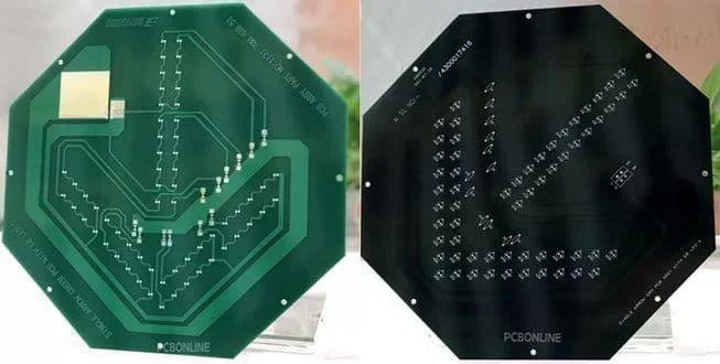
Examples of double-sided FR4 PCB design
1. Industrial control PCB: MCU, R/C components, and interface chips on the top layer, terminal blocks, and relays on the bottom layer. Features: Robust structure, maintainable.
Power supply PCB: Control chips, small MOSFETs on the top layer, large inductors, large capacitors, and pin headers on the bottom layer. Features good heat dissipation.
Consumer electronics PCB: SMDs on the top layer, USB and battery holder on the bottom layer. Features include space-saving and automation.
FR4 double-sided PCB design for complex circuits
A complex double-sided FR4 PCB consists of an FR4 insulating substrate with ≥2 copper layers. Its PCB design features multiple signal layers, via interconnects, ground partitioning, and high-density routing.

A structure of a complex double-sided FR4 PCB can be:
- Top layer: Signal traces + SMDs.
- Internal power/ground layers
- Bottom layer: Signal traces, ground traces, power return paths.
A complex double-sided FR4 PCB requires two SMT reflow soldering cycles, first reflow for high-density SMDs and second reflow for the secondary side. Keep in mind these considerations in a complex double-sided FR4 PCB design.
- Routing: route the top layer horizontally and the bottom layer vertically to reduce trace crossovers. Reserve via areas during the routing phase to prevent signal blockage.
- Via and interconnect: If a signal layer is adjacent to a power layer, control the via annular ring size and spacing to prevent electrical coupling interference. Critical high-speed signals should minimize the number of vias to avoid reflections and impedance discontinuity.
- Power and ground: A hybrid approach of local power islands combined with poured ground copper is common. Connect the top and bottom ground copper with multiple vias. Use local ground planes or ground mesh in high-speed device areas to ensure stable signal referencing. Place decoupling capacitors between power and ground, positioning them as close as possible to the chip's power pins.
- Analog signal design: Matching impedance with trace width based on FR4 dielectric constant of 4.2-4.8. Maintain critical differential pairs symmetry and consistent spacing. Avoid routing signals across split plane regions. Establish separate ground lines for analog and digital areas, converging at a single point.
- Thermal management: Control the second reflow temperature profile to prevent component oxidation or unsoldering. Enhance heat dissipation through copper pour extensions and thermal via arrays. Located high-power devices near the PCB edge or adjacent to heat-dissipating copper areas.
- Spacing: Via to pad ≥ 8mil, trace width/spacing ≥ 4mil. Reserve test points to facilitate functional testing of the dual-layer circuitry.
FR4 Double-sided PCB Assembly
If a double-sided FR4 PCB has surface-mount components on both sides, it needs to pass through the SMT production line twice. At PCBONLINE, our double-sided PCB assembly service ensures that the components on the first side do not drop off, oxidize, or suffer thermal damage during the second reflow cycle.
During double-sided FR4 PCB assembly, we first place SMDs and apply red adhesive dots on the Bottom Layer with fewer or bulkier components.
Then we complete the bottom side soldering with reflow soldering for the first time.
Next, we print solder paste and place components on the Top Layer and complete top-side soldering. Here, the PCBA passes through the reflow oven for the second time.
If the double-sided FR4 PCB also requires THT soldering, we insert the component leads and wave solder.
During the second reflow, risks such as component drop-off and oxidation may happen. How do we control the PCBA process to prevent potential risks? Below is how we do.
- 1. Fix back-side components with red adhesive and limit the weight to < 30mg/component of the bottom-side. This is to prevent heavy components from falling due to gravity when facing down in the oven.
- 2. Control ramp-up rate ≤ 3℃/s and cooling rate ≤ 6℃/s. This is to prevent thermal shock, which can cause micro-cracks in components or pads.
- Use nitrogen reflow soldering to prevent solder joints from yellowing or tin oxidation.
- 3. We control reflow/wave oven temperature precisely to prevent solder maste smearing and other thermal-related issues.
- 4. Appropriately reduce airflow speed to prevent component shifting, and use red adhesive for fixation.
PCBONLINE has rich experience in reflow/wave oven temperature control. Our CAM engineers design the reflow profile custom for each double-sided FR4 PCBA. A typical reflow temperature profile is like:
- Reflow peak temperature: 230℃ ~ 250
- Time control: Pre-heat zone 90s - 120s, reflow zone > 220℃ 30s - 60s, cooling zone avoiding rapid quench
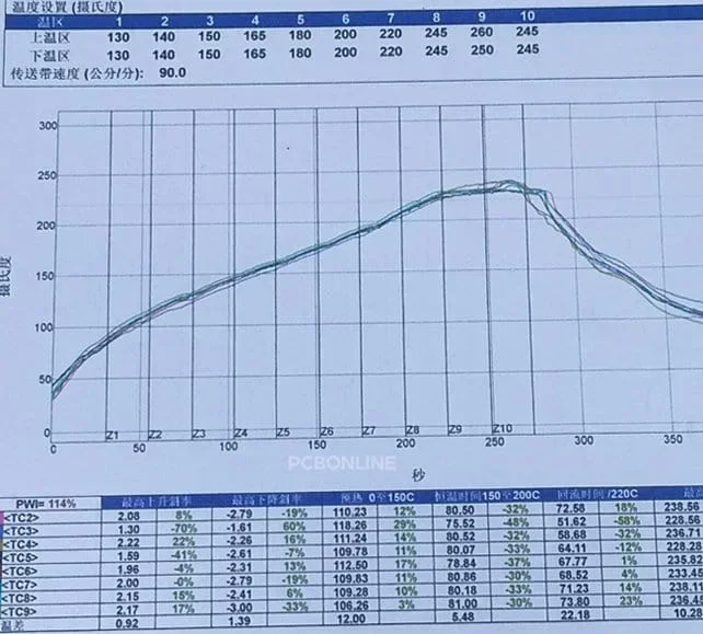
During the second reflow, a slightly lower peak temperature is used to reduce thermal shock. For example, 245℃ for the first pass and 235℃ for the second.
Post-assembly services
After SMT and THT assembly, PCBONLINE can conduct complete post-assembly value-added services:
- In-circuit testing for short/open detection
- Functional circuit testing to verify operational performance
- Burn-In testing for thermal and electrical reliability
- Conformal coating to protect the PCBA from moisture, dust, and corrosion
- IC programming for transferring your program into the bare IC before delivery
- Box-build assembly to install the PCBA in the enclosure to become the final device

Partner with PCBONLINE for Turnkey FR4 Double-sided PCB
Since the foundation in 2005, PCBONLINE has been committed to turnkey OEM PCBs, including FR4 two-sided PCBs. We focus on PCBA manufacturing from prototypes to mass production. We can also provide box-build assembly to the PCBA, a module, and the final device.
Our turnkey OEM PCBA services offer:
- Turnkey PCBA manufacturing: From PCB ptototypes and testing to mass PCBA and box-build assembly, our PCB assembly services are custom and one-stop.
- Complete procurement: We source and customize enclosures, cables, and accessories from reliable suppliers.
- Engineering support: We check enclosure and accessory designs for compatibility with your PCBA and can suggest design changes.
- Free DFM/DFT: We provide free Design for Manufacturability (DFM) and Design for Testability (DFT) checks to ensure that designs are optimized for a smooth production process.
- Quality assurance: IPC-A-610 Class 2/3, automotive-grade or industrial-grade inspection standards.
- Turnkey delivery: From PCB fabrication to final product packaging and shipping.

PCBONLINE manufactures, assembles, and tests PCBs and PCBAs to box builds as a source factory manufacturer under one roof, from prototypes to bulky production, saving costs and time for you.
We have powerful manufacturing strength for advanced PCBs and high-end assemblies, such as HDI PCBs, high-frequency PCBs, ceramic PCBs, waterproof sealing, and 01005 fine-pitch assembly.
We can precisely control reflow/wave oven temperatures, design PCBA fixtures, and help create user manuals, installation guides, and compliance labels.
Our high-quality PCBA contract manufacturing is certified with ISO 9001:2015, ISO 14001:2015, IATF 16949:2016, RoHS, REACH, UL, and IPC-A-610 Class 2/3.
Our one-on-one free and professional DFM helps you debug and improve design, to ensure the manufacturability, cost-effectiveness, and final device success.
Whether you need double-sided FR4 PCBs for industrial controls, AI hardware, IoT devices, medical-grade products, automotive modules, etc, we can deliver the PCBAs and modules of high quality and in time, meeting any of your project requirements. To get a quote for your PCBA or custom module project, email us at info@pcbonline.com.
Conclusion
We offer double-sided FR4 PCBs of medium and complex circuits. With more than 20 years of electronic manufacturing experience in turnkey OEM PCBA, we are ready to check your Gerber and provide turnkey services for your double-sided FR4 PCB project. Contact PCBONLINE today!
PCB fabrication at PCBONLINE.pdf
PCB assembly at PCBONLINE.pdf


