
PCB on PCB designs save space for compact devices and allow for modularity. There are many creative ways to connect two or more printed circuit boards - as long as the design can work. With 20 years of expertise in PCB manufacturing and PCB assembly, PCBONLINE shares four essential PCB-on-PCB design solutions in this article —
For each PCB-to-PCB solution, we have manufactured them and will provide their pictures and content below for your clear understanding. We hope these insights will inspire and illuminate your PCB and modular design.
1. Using Brass Standoffs to Stack the PCBs
The stacking PCB on PCB method uses connectors and mechanical standoffs to mount a daughter board on top of a motherboard.
Pin headers are typical connectors to provide electrical connections.
Brass standoffs ensure mechanical stability and maintain a precise gap between boards.
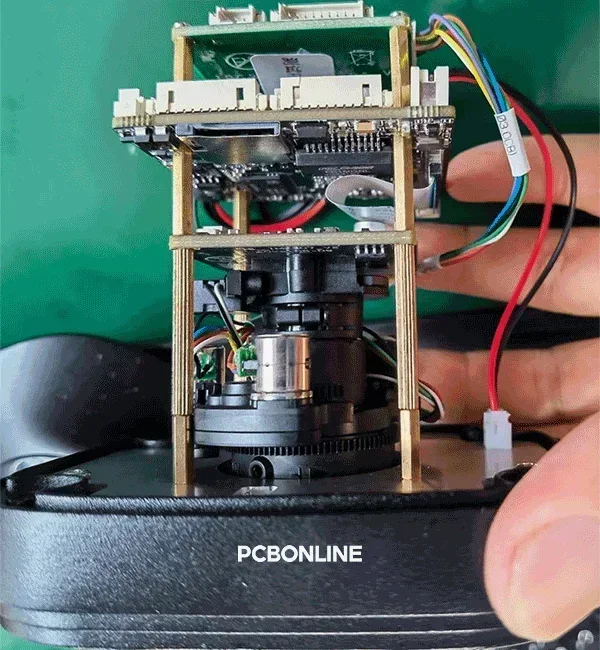
The stacking PCB-on-PCB method offers design flexibility. Modules can be easily swapped, and testing individual boards is simple. It helps product upgrades, reduces assembly complexity, and simplifies troubleshooting.
Consider an embedded system. The main processing board serves as the motherboard. A separate display board can be a daughter board. Pin headers connect the two. This setup is highly modular. It allows different display types to be used with the same main board. USB ports, Ethernet ports, and other peripherals remain on the motherboard.
The benefits of using connectors and standoff to stack PCBs are clear —
- Modularity: Systems can be easily expanded. Various functions can be added or changed.
- Extend product lifespan: This approach allows for future upgrades.
- Simplified servicing: Field servicing becomes easier.
- Easy testing: Individual boards can be tested simply.
However, stacking PCB-on-PCB adds height, so the total device profile increases. This can be a concern for very thin products. Signal integrity can also be affected as long pin headers may introduce impedance issues, especially for devices at high frequencies.
For low-profile stacking, specialized PCB on PCB connectors exist. These include high-density, low-profile connectors like Hirose or Molex. They reduce the gap between boards. This mitigates some height and signal concerns. Another robust stacking method uses SMT receptacles on the top PCB. Thru-hole pin headers pass through both boards and are hand-soldered. This creates a very strong connection.
2. Using connectors to lift the vertical daughterboard on the main board
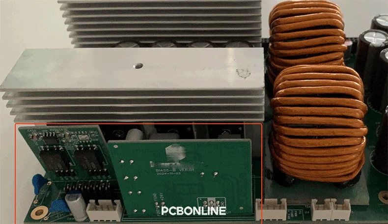
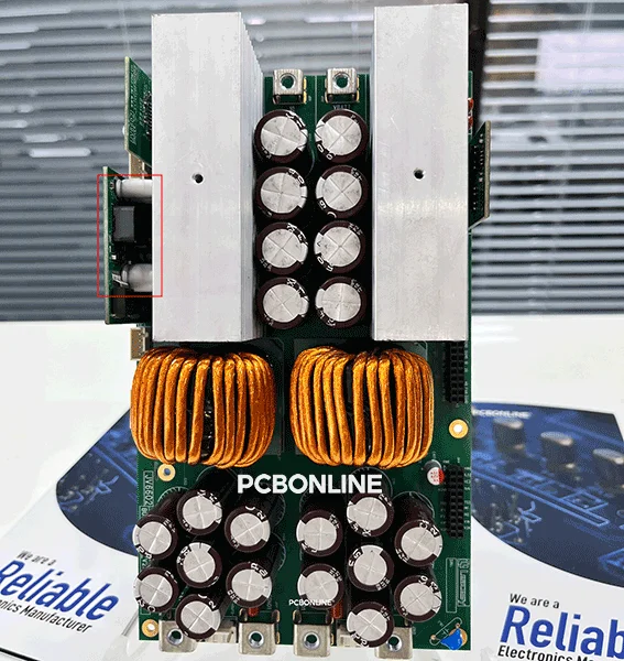
In the stacking PCB on PCB method, the main board and daughter board are in the same horizontal orientation. By contrast, in this PCB-on-PCB method also uses connectors, the daughter board connects to the motherboard perpendicularly. The smaller PCB stands upright, at a 90-degree angle to the main board.
The lifting up daughterboard vertically approach uses right-angle connectors to provide both electrical and mechanical connections. This configuration is visible in many high-power and industrial electronics. For example, the above picture is one of our high-power PCBA for industrial controls.
This PCB-on-PCB method offers a unique benefit:
- Optimal space utilization: It makes efficient use of board spaces. Instead of adding to the height of a stack, it extends the width or length. A narrow enclosure can benefit from components standing upright rather than lying flat.
- Enhanced component clearance: Vertical mounting can provide more breathing room for components. This is especially true for tall parts like large capacitors or heat sinks on either the daughter or the motherboard. So yeah, our above PCBA picture perfectly illustrates this point.
- Direct access to ports/connectors: In some cases, vertically mounted boards serve as I/O panels. They can directly present ports (like USB, Ethernet, or audio jacks) to the edge of an enclosure. This simplifies product design and user access.
- Improved airflow: In some designs, vertical orientation can aid in thermal management. It might allow for better airflow across the surfaces of both PCBs. This helps dissipate heat more effectively.
However, if you use the connectors to connect the daughterboard perpendicularly to the main board, consider the following factors —
* Increased footprint: While saving height, it increases the overall width or length of the combined assembly.
* Mechanical stress: The single connection point might experience more leverage or stress from impacts. Secure mounting, often with additional mechanical supports or standoffs, is important. That's why PCBONLINE uses standoffs for the other vertical daughter in the picture below, shot for the same high-power PCBA.
* Connector specificity: This method requires specific vertical or right-angle connectors. These can sometimes be more specialized or costly than standard pin headers.
Besides high-power applications like industrial control systems, vertical PCB-on-PCB connections also find uses in network equipment like computing modules. This PCB-on-PCB method is ideal when height is limited but horizontal space is available. It offers a clever way to integrate functionality into compact designs.
3. Using edge castellations (half holes) to solder the daughterboard to the main board
Edge castellations, also known as half holes, provide a PCB-on-PCB solution by soldering the daughterboard from its plating half holes at the edge to the main board. These plated half-holes on the edge of a daughter board are PCB outline cut through plated through-holes. This leaves a series of half-cylinders. These exposed, plated surfaces act as solder pads.
The daughter board is then soldered directly onto a motherboard. It functions much like a large surface-mount device (SMD). This method creates a very compact connection. It eliminates the need for bulky connectors. The daughter board becomes an integrated component.
This approach is highly favored for miniaturization. Think of IoT modules. Wireless modules (Wi-Fi, Bluetooth) often use castellations. They are directly soldered onto the main PCB board. This saves valuable space. It reduces the overall footprint.
Advantages of using edge castellations for soldering PCB on PCB include —
- Space efficiency: Maximizes space by eliminating bulky connectors.
- Robust connection: Direct solder connection offers excellent mechanical strength. It resists vibration well.
- Improved electrical performance: Shorter signal paths minimize loss and interference.
- Streamlined manufacturing: Automated pick-and-place machines can handle these modules. This reduces manual assembly time.
However, rework of the half-hole PCBs can be challenging. Once soldered, separating the boards is difficult as the connection is not designed for frequent detachment. Careful design and proper castellation manufacturing are critical. PCBONLINE has rich experience in manufacturing and assembling half-hole PCBs can also help you ensure the design manufacturability and optimize it. Sometimes, flexible glue is used along one edge to relieve mechanical stress and improve long-term reliability.
4. Inlaying the daughter board into the main board and soldering the raw PCBs before PCB assembly
The inlay method offers a unique form of PCB on PCB design: A daughter board is embedded into a cutout on the motherboard. The daughter board fits snugly into this recess. Then, the raw PCBs are soldered together before component assembly and reflow.
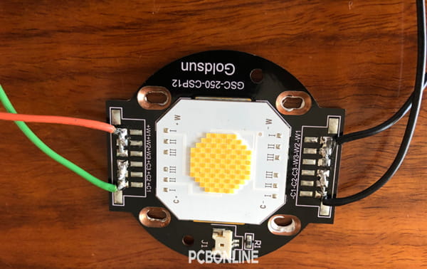
This method achieves an extremely low profile. The daughter board sits flush with or slightly below the motherboard's surface. It can create a seamless appearance. This is ideal for thin devices. For example, the above high-power LED light PCBA was manufactured by PCBONLINE. The daughterboard is a ceramic PCB, and the main board is a copper-core PCB. The COB LED light source is then assembled on the ceramic daughter board.
Consider high-power LED applications. Ceramic PCBs are often used for LEDs. They have superior thermal conductivity. A ceramic daughter board can be inlaid into a copper-based motherboard. The ceramic board holds the COB (Chip-on-Board) LEDs. This combination provides excellent heat dissipation. It ensures a long LED lifespan. The direct soldering connection creates an efficient thermal path.
The benefits of inlay/embedding the daughterboard into the main board include —
- Superior thermal management: Heat transfers efficiently from the daughter board to the motherboard. This is crucial for power electronics. It benefits high-brightness LEDs.
- Incredibly robust connection: Withstands mechanical stress well.
- Maximized space utilization: Achieves extremely low profiles.
However, the inlay method demands high precision. Manufacturing tolerances must be tight. The cutout on the motherboard must perfectly match the daughter board. Rework is extremely difficult. Once soldered, separating the boards is almost impossible without damaging components. This method is best for designs with high production volumes. It suits applications where long-term reliability is paramount.
Some advanced inlay techniques resemble BGA (Ball Grid Array) packages. Here, the top PCB has pads on its bottom surface. These are soldered onto corresponding pads on the bottom PCB. This creates a minimal gap. Coplanarity is critical for such designs. Ensuring both PCBs are perfectly flat during reflow is challenging. Any warpage can lead to unreliable connections.
Besides the above PCB-on-PCB solutions, what's your idea? Feel free to communicate with PCBONLINE by filling out the table on the right. Choosing which method for your PCB-on-PCB project depends on many factors:
- space constraints
- thermal requirements
- signal integrity needs
- cost
- PCB assembly process
- repairability
- desired modularity.
Partner with PCBONLINE for PCB-on-PCB Solution, One-stop Manufacturing
From concept to mass production, PCBONLINE is your trusted partner for PCB-on-PCB solutions. We offer comprehensive PCB manufacturing and assembly services and can handle all types of PCB on PCB designs.
Founded in 2005, PCBONLINE has two large advanced PCB manufacturing bases, one PCB assembly factory, stable supply chains, and an R&D team.
We are proficient in producing stacked PCBs with connectors and standoffs. We ensure precise pin header alignment.
We excel in complex inlay designs, including working with diverse materials like ceramic, copper-core, and FR-4.
Our aperture range of daughter PCB half holes is 0.5mm to 1.2mm, and the center-to-center distance range between adjacent half holes is 0.75mm to 1.27mm.
Our team provides one-on-one engineering support and ensures your PCB on PCB design is manufactured with precision.
Microvias can be made as single microvias, staggered vias, stacked vias, and skipped vias.
High-quality PCB and PCBA manufacturing certified with ISO 9001:2015, ISO 14001:2015, IATF 16949:2016, RoHS, REACH, UL, IPC-A-600 Class 2/3, and IPC-A-610 Class 2/3.
PCBONLINE manufactures, assembles, and tests PCBs and PCBAs to box builds as a source factory manufacturer under one roof, from prototypes to bulky production, saving costs and time for you.
Whether you need a PCB-on-PCB stacked solution, a compact castellated module, or a robust inlaid assembly, PCBONLINE delivers. Whether you need a PCB-on-PCB stacked solution, a compact castellated module, or a robust inlaid assembly, PCBONLINE delivers. If you want to get a quote or ask questions, you can send emails to info@pcbonline.com.
Conclusion
This article explores four main methods for PCB on PCB integration. These are inlay, perpendicular connecting, stacking, and edge castellations. Experience unparalleled quality and service from PCBONLINE. Let us bring your innovative PCB on PCB design to life.
PCB fabrication at PCBONLINE.pdf


