
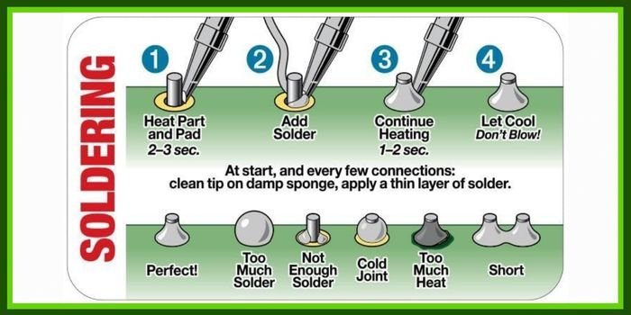
As one of the most important standards in the electronics industry, IPC-A-610 provides comprehensive visual quality guidelines for the acceptability of electronic assemblies. For those engaged in electronics manufacturing, quality control or training, it is essential to understand the basic concepts and requirements of IPC-A-610. This article will explore the relevant issues of IPC-A-610 welding standards in depth through a question-and-answer format.
In this article:
Part 1.What is IPC-A-610? Part 2.Why is IPC-A-610 so important? Part 3.What quality issues does IPC-A-610 focus on? Part 4.Three classes of IPC-A-610 Part 5.How can manufacturers learn and apply IPC-A-610?What is IPC-A-610?
IPC-A-610 (Acceptability of Electronic Assemblies) is an industry standard published by the Association Connecting Electronic Industries (IPC). It provides detailed guidance on the visual quality requirements of electronic assemblies, especially solder connections. In simple terms, it defines the appearance standards of good, acceptable, and defective electronic assemblies, helping manufacturers, suppliers, and customers to unify their understanding of product quality.
Why is IPC-A-610 so important?
IPC-A-610 is important in many ways: It unifies industry standards by establishing a common quality assessment framework for the global electronics industry, ensuring that components from different companies and regions can achieve consistent quality levels. By following the requirements of IPC-A-610, companies can effectively reduce product failures caused by soldering defects and significantly improve product reliability and life. In addition, clear quality standards help to detect and correct problems early in production, reducing unnecessary rework, repair costs, and product scrap. It also provides a common set of terminology and visual references to promote clear communication between manufacturers, inspectors, and customers about quality requirements, and is the basis of many training and certification courses in the electronics industry, ensuring that practitioners have the correct soldering and inspection skills.
What quality issues does IPC-A-610 focus on?
IPC-A-610 focuses on visual inspection of electronic assemblies and covers several key areas. At its core are detailed regulations for solder joint quality, including the shape, wettability, surface finish, and the presence or absence of cracks or voids, as well as acceptable and unacceptable features, for various types of solder joints (e.g., through-hole solder joints, surface mount solder joints). The standard also specifies requirements for component mounting in detail, such as component location, orientation, flatness, lead bend, and alignment with pads. In addition, it also covers specifications for wires and terminations, such as wire stripping lengths, solder connections, and strain relief. Board cleanliness is another important aspect, and the standard specifies flux residues and contaminants, while also covering the evaluation of possible mechanical damage to boards, components, pads, etc., and provides some guidance on the acceptability of rework and repair operations.
Three classes of IPC-A-610
IPC-A-610 classifies electronic components into three product classes, which are designed to reflect the intended use of the product and the required reliability level.
Class 1: Applicable to general electronic products, such as consumer electronics, focusing mainly on functionality, allowing a certain degree of defects as long as they do not affect basic functions.
Class 2: For electronic products that require continuous performance and uninterrupted service, such as industrial control and communication equipment, with higher quality requirements, but still allowing some cosmetic defects that do not affect long-term reliability.
Class 3: Applicable to electronic products with high performance, high reliability or operating in harsh environments, such as medical, aerospace and military equipment, with extremely strict quality requirements, almost no cosmetic defects are allowed, and the highest reliability and life are emphasized. In actual production, it must be clearly specified which product class should be followed based on the end use of the product and customer requirements.
How can manufacturers learn and apply IPC-A-610?
For a manufacturer, mastering the production capacity of IPC-A-610 standard will undoubtedly improve its core competitiveness and bring other benefits. For welding operators, quality inspectors and engineers, mastering IPC-A-610 knowledge can significantly improve their professional skills and industry competitiveness. Enterprises can establish and optimize production and inspection processes based on this standard, thereby standardizing production processes and ensuring the consistency and controllability of product quality. By reducing rework and scrap, production costs can be effectively reduced, and production efficiency can be improved. In addition, a quality system that meets international standards can significantly enhance the image and trust of the company in the minds of customers. As an internationally recognized standard, following IPC-A-610 can also help companies promote international trade and better participate in global market competition.
The IPC-A-610 standard not only specifies the requirements for solder joint quality, component installation, cleanliness, etc., but also divides them into three different categories according to the intended use and reliability requirements of the product. In-depth understanding and application of IPC-A-610 can significantly improve product reliability, reduce production costs, promote international trade, and provide professional training and certification for individuals and companies. It is the key to ensuring the high quality and high performance of electronic products.
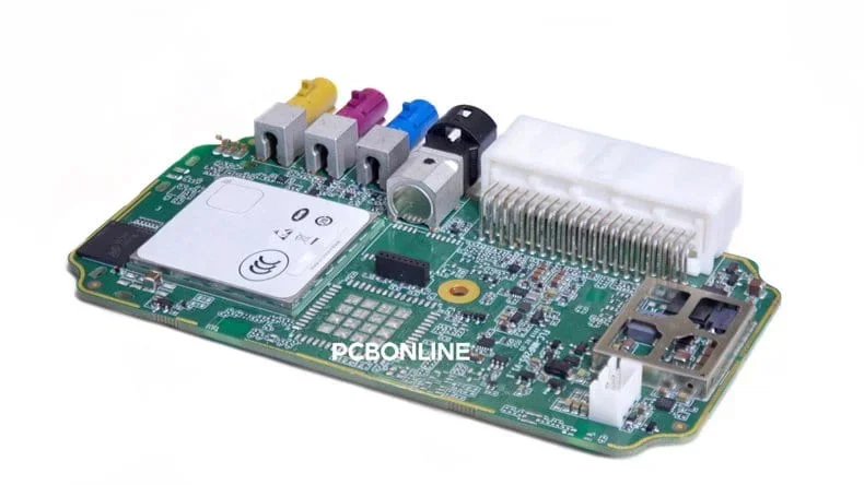
One-Stop HDI PCB Manufacturer and Its PCB Via Filing Capabilities
If you're looking for turnkey HDI electronics manufacturing services (EMS) from hardware development to PCBA fabrication and box-build assembly, you can work with the one-stop HDI PCBA manufacturer PCBONLINE.
Founded in 1999, PCBONLINE has R&D capabilities for HDI projects and EMS manufacturing capabilities, including via filling for stacked vias. It provides 4-to-64-layer HDI PCB fabrication, assembly, and PCBA box-build assembly. You can order various HDI PCBs from PCBONLINE, such as FR4, polyimide (flexible PCB), polyimide + FR4 (rigid-flex PCB), and PTFE/Rogers (high-frequency PCB).

3000m² of production capacity per day for HDI PCBs with builds of 1+N+1, 2+N+2, 3+N+3,4+N+4, and arbitrary interconnection in any layers.
PCBONLINE has hardware and software R&D capabilities for IoT applications requiring HDI design, including PCBA and enclosures.
We can manufacture complex PCBs with stacker vias, via-in-pad, microvias, inlay boards, heavy copper designs, and hybrid and fine structure lay-ups.
Besides HDI PCB fabrication, we have powerful capabilities in fine-pitch assembly for HDI PCB assembly.
We have rich R&D and manufacturing experience for HDI applications such as FPGA boards.
High-quality HDI PCB and PCBA manufacturing certified with ISO 9001:2015, IATF 16949, RoHS, REACH, UL, and IPC-A-610 Class 2/3.
Here'e the PCB via filing capabilities at PCBONLINEL:
- Micriavia filling with copper: laser via size 0.1-0.125mm, priority 0.1mm
- Finished hole size for via-in-pad filling with resin: 0.1-0.9mm (drill size 0.15-1.0mm), 0.3-0.55mm normal (drill size 0.4-0.65mm)
- Max aspect ratio for via-in-pad filling with resin PCB - 12: 1
- Min resin plugged PCB thickness: 0.2mm
- Max via-filling ith resin PCB thickness: 3.2mm
- Making different hole sizes with via filling in one board: Yes
- Via filling with copper/silver: Yes
If you need HDI PCBAs or any other PCBAs requiring via filling, please send your email to PCBONLINE at info@pcbonline.com. We will provide one-on-one engineering support to you.
Conclusion
Via filling is used for creating stacked vias in HDI PCB fabrication, BGA/CSP/QFN IC packaging, and filling PCB via-in-pad with resin during multilayer PCB fabrication. If you need one-stop electronics manufacturing for your HDI PCBA project, contact the one-stop advanced PCB manufacturer PCBONLINE for high-quality PCBA and box-build solutions tailored to your project's needs.
PCB fabrication at PCBONLINE.pdf


