

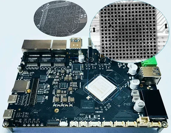
Most HDI PCB designs use fine-pitch BGAs. At 0.4mm or 0.35mm pitch, signals cannot conventionally escape the package. There is not enough room between pads for dog-bone fan-out, so the design needs microvias and via-in-pad structures to route the nets out.
Getting that PCB manufactured does not complete the project. Most HDI projects do not fail at fabrication but later, when those BGAs are assembled and their solder joints verified. A voided via fill, a marginal surface finish, or a PCB that warps in reflow can turn a sound design into an intermittent field failure.
This article follows the chain from PCB fabrication to final test, and notes the decisions where fine-pitch BGA designs most often go wrong. At PCBONLINE, we manufacture, assemble, and test PCBs under one roof.
Via-in-Pad: Why Copper Filling Has to Be Void-Free
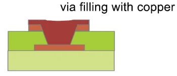
At 0.4mm pitch, adjacent BGA pads sit about 0.2mm apart. Between them, there is no room for a via plus a trace, so the classic dog-bone fan-out does not fit. The via has to go directly into the pad, and we call the structure via-in-pad (VIP).
VIP creates a requirement that the pad must behave like a solid pad. Solder paste has to print evenly across it, and the BGA ball has to land on a level surface. So the via cannot be left open. In the HDI manufacturing process, the laser-drilled microvia is plated, filled solid with electroplated copper, and planarized flat. The finished structure follows IPC-4761 Type VII, filled and capped with plated copper.
Two factors determine whether microvia copper filling works:
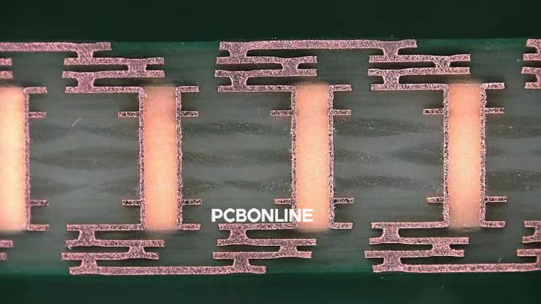
Void-free fill. A void inside a via-in-pad traps air. When the PCB goes through reflow at 240°C to 260°C, that air expands and stresses the surrounding copper; over thermal cycles, the copper can crack. A void under a BGA pad can also let the pad surface deform or sink slightly, so the ball never makes full contact. The symptom is an intermittent connection. It passes initial testing and fails in the field.
Plated copper thickness. The via barrel needs about 15μm to 25μm of plated copper to carry current and hold up mechanically, and the cap over the fill needs enough thickness to stay flat and durable. We verify both with cross-section microsectioning, cutting a sample via, polishing it, and measuring the copper under a microscope. X-ray provides a non-destructive check for voids in the fill.
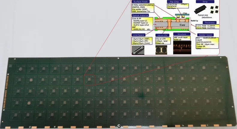
Assuming the pad comes out flat, the next question is what surface finish sits on it, because the finish decides how the solder wets in the PCB assembly process.
Surface Finish for BGA Pads: ENIG or ENEPIG?
The surface finish on BGA pads strongly affects solder joint quality. For HDI PCBs with fine-pitch BGAs, the reliable finishes are ENIG and ENEPIG.
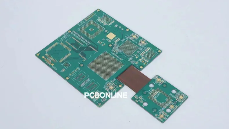
ENIG (electroless nickel immersion gold) is the standard finish for BGA pads. The nickel layer blocks copper from diffusing into the solder, and the thin gold layer keeps the nickel from oxidizing during storage. It is flat, solderable, and the usual choice for commercial and industrial HDI PCBs with BGA, QFN, and fine-pitch SMDs.
ENEPIG (electroless nickel electroless palladium immersion gold) inserts a palladium layer between the nickel and the gold. Its job is to prevent nickel corrosion, a failure mode where the nickel surface oxidizes during reflow and weakens the joint. So ENEPIG is the safer choice when the PCB will see multiple reflow cycles, when wire bonding happens alongside assembly, or when the product targets high-reliability sectors such as medical, aerospace, automotive, or military. The palladium layer also improves solder joint ductility compared with ENIG.
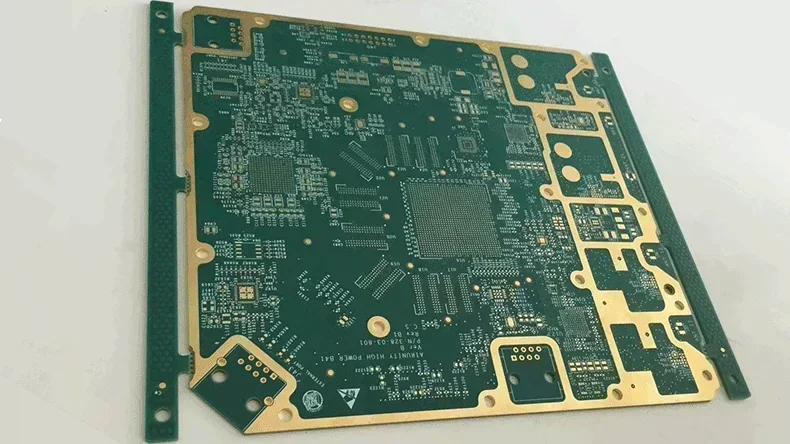
Microvia flatness matters as BGA balls at 0.35mm pitch are tiny. They run 0.15mm to 0.25mm in diameter, and any pad irregularity, whether from a poorly filled via or from finish plating variation, changes how the ball wets and forms the joint. ENIG and ENEPIG both deliver the coplanar surface that fine-pitch assembly requires.
Which finish should your HDI BGA design use? For a single-reflow commercial product, ENIG is enough. If the PCB faces a harsh thermal environment or needs wire bonding, choose ENEPIG. And if you are designing at 0.35mm pitch and are not sure, send your stack-up and reflow plan to our engineering team, and we will give you a straight answer.
A reliable surface finish on a flat pad is only as good as the PCB underneath it. Warpage undoes everything covered so far, which is why it is the next thing to control.
HDI BGA PCB Warpage Control
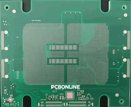
BGA solder joints are short. A 0.4mm pitch BGA with 0.3mm balls forms joints about 0.15mm to 0.2mm tall after reflow. With PCB warpage of 0.1 mm across the BGA footprint, some balls will not touch their pads.
Warpage is the most common BGA assembly failure on HDI PCBs, and it is usually built in before the PCB reaches the SMT line.
The causes of PCB warpage are below:
- Uneven copper distribution across the layers creates uneven thermal expansion during lamination.
- Material mismatch. High-Tg FR-4 cores need matched-CTE prepregs; mixing material sets makes the PCB curl as it heats.
- Sequential lamination stress. HDI's multiple press cycles add stress, and poorly controlled press parameters leave it locked into the finished PCB.
- Thin PCBs warp more. Below 0.8mm, warpage becomes more severe.

IPC-6012 sets the SMT bow-and-twist limit at 0.75% of the PCB's longest diagonal (measured per IPC-TM-650 2.4.22). For a 100mm PCB, the limit works out to 0.75mm, acceptable for standard components but far too much for a fine-pitch BGA. At 0.35mm pitch with 0.15mm joints, the practical tolerance across the BGA footprint is often under 0.05mm.
At PCBONLINE, we measure flatness on every HDI panel before it enters the SMT line. Panels that exceed the warpage limit for the components they carry go back for rework or are rejected.
Once the PCB is flat and the finish is chosen, the SMT line takes over.
HDI PCB BGA Assembly: What to Control on the Line
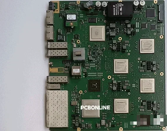
An HDI PCB with fine-pitch BGAs require PCB assembly with precision.
At PCBONLINE, our turnkey PCB assembly factory runs four fully automated SMT lines. All of them support HDI PCB assembly, with a finest component pitch of 0.35mm, enough for FBGA, fine-pitch QFN, and 01005 (0.4 × 0.2mm) and 0201 (0.6 × 0.3mm) passives.
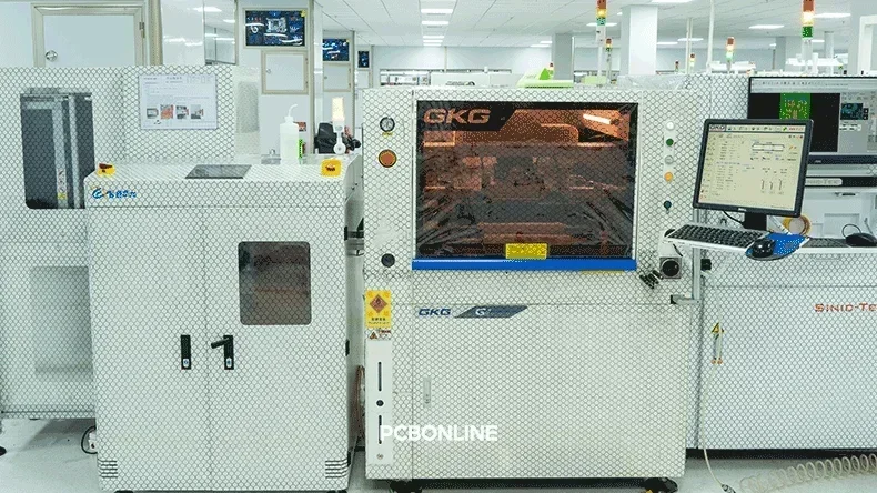
Solder paste printing decides joint quality. We run 3D SPI (solder paste inspection) on every SMT line: the machine measures paste volume, height, and position on every pad. It catches stencil and printing issues before SMD pick-and-place.
Our SMD placement uses vision alignment to the PCB fiducials. For BGAs, the machine also aligns to the ball pattern on the package itself, compensating for package-to-package variation in ball position.

Reflow soldering follows SMD placement and pre-reflow automatic optical inspection (AOI). Peak temperature, time above liquidus, and ramp rate control how the joints form. We profile every HDI PCB with thermocouples attached at the BGA locations.
After reflow soldering, PCBA testing and inspections find out whether the solder joints formed correctly.
HDI BGA Testing and Inspection
3D AOI runs before and after reflow. Pre-reflow, it checks solder paste print and placement accuracy, catching issues before they become reflow defects. Post-reflow, it inspects visible joints, component orientation, and polarity.
BGA joints sit under the package out of sight, so the AOI inspection can't verify the BGA soldering quality.
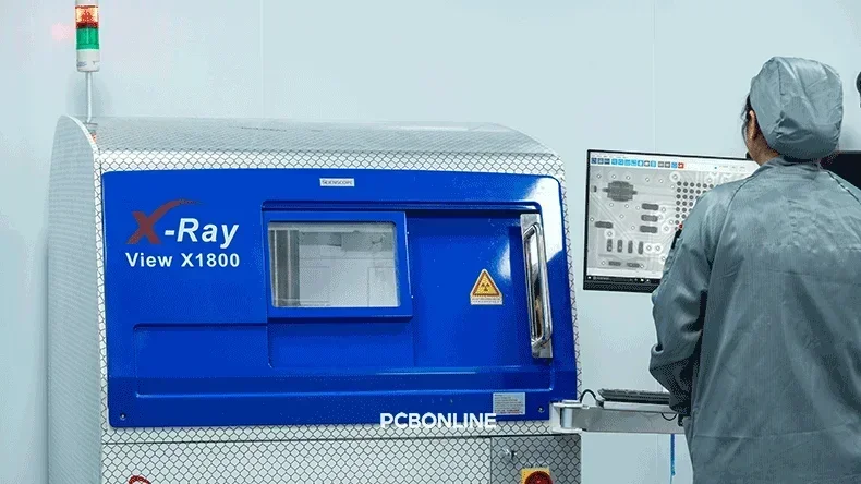
X-ray is used for BGA joint verification to look through the soldering joints and microvias via-in-pad fills. It images the solder joints through the package, and 3D X-ray can isolate individual balls.
We look for voids in the solder, head-in-pillow defects (the ball sitting on the paste without merging), cold joints from insufficient wetting, and shorts between adjacent balls. A void in the via-in-pad copper fill also shows up clearly in the image.
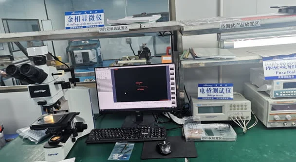
After HDI PCB assembly, we also run a cross-section microsection. We cut sample PCBs, mount them in resin, polish the cross-section, and inspect under a microscope to confirm via-in-pad fill quality, barrel copper thickness, and interlayer connection integrity. For any new HDI projects and process changes, we run a cross-section verification before production continues.
Besides, we have a first article inspection for prototype and sample orders. We randomly pick up a prototype board to check every component against the BOM, confirming correct value and tolerance, and send the report for customer approval before volume production starts.
In summary, HDI PCB assembly requires filling the microvias properly, choosing a reliable finish for the environment, keeping the PCB flat, controlling the paste, and testing the HDI PCB assembly comprehensively.
Collaborate with PCBONLINE for HDI BGA PCB Assembly
PCBONLINE provides turnkey HDI PCB manufacturing and assembly under one roof with fine-pitch capabilities down to 0.35mm, meeting fine-pitch BGA and QFN assembly requirements easily.

Founded in 2005, PCBONLINE has four locations for HDI PCB manufacturing and assembly — two large advanced PCB manufacturing bases in Jiangsu and Jiangxi Provinces in China, one turnkey PCB assembly factory in Shenzhen, and a smart OEM center and headquarters also in Shenzhen.

Our HDI capabilities include stack-ups from 1+N+1 to 4+N+4, any-layer HDI, up to 64 copper layers, laser microvias down to 0.075mm, trace width/space control within ±0.02mm, and impedance control within ±2%.
Before any material is purchased, our engineering team performs a full DFM analysis covering microvia design, stack-up structure, trace width and spacing, impedance requirements, and manufacturing feasibility.
At our PCB assembly factory, PCBONLINE runs four fully automated SMT lines with 3D SPI, dual-stage 3D AOI, X-ray inspection for BGA and hidden-joint components, and first article inspection reporting on prototype orders.
Our combination of fine-pitch BGA assembly and X-ray inspection verifies both the microvia connections underneath the BGA and the BGA solder joints themselves.
Our experienced engineers provide one-on-one engineering support, solving technical and non-technical challenges while offering optimization suggestions to ensure your project runs smoothly from start to finish.
High-quality HDI PCB manufacturing certified with ISO 9001:2015, ISO 14001:2015, IATF 16949:2016, RoHS, REACH, UL, and IPC-A-600 Class 3.
Whether you need HDI PCB manufacturing and assembly to build AI servers, GPU boards, high-speed network equipment, or medical-grade systems, with 21 years of HDI PCBA manufacturing experience, we ensure that both electronics performance and final product presentation meet the highest standards. To get a quote for your HDI PCB project from prototype to bulk production, send your Gerber to info@pcbonline.com.
FAQ about BGA HDI PCB
Q: What is via-in-pad, and why does it need copper filling?Via-in-pad places the via directly in the BGA pad. At 0.4mm pitch and below, there is no room for dog-bone fan-out, so the via must go in the pad. Copper filling and planarization make the pad behave like a solid pad, so solder paste prints evenly and the ball lands flat. Without filling, solder paste would wick down into the via hole during reflow, leaving too little solder on the pad and causing weak or open joints.
Q: What is the difference between ENIG and ENEPIG for BGA pads?ENIG (electroless nickel immersion gold) is the standard finish for BGA assembly. ENEPIG adds a palladium layer between the nickel and gold, which prevents nickel corrosion and improves solder joint ductility. ENIG is sufficient for most commercial HDI PCBs; ENEPIG is specified for high-reliability applications, multi-reflow processes, or designs that need wire bonding alongside BGA assembly.
Q: Why does PCB warpage cause BGA assembly failures?Fine-pitch BGA solder joints are only 0.15mm to 0.2mm tall. If the PCB warps by more than that across the BGA footprint, some balls cannot reach their pads. Corner balls lift off, or center balls never touch. Warpage must be controlled during manufacturing and measured before assembly, because reflow will not flatten a warped PCB.
Q: Can X-ray detect voids in via-in-pad copper filling?Yes. X-ray reveals voids in the copper fill underneath BGA pads, and it is non-destructive. Cross-section microsection gives the most direct measurement of fill quality and copper thickness, which is why high-reliability HDI programs use both: X-ray on production panels and cross-section on sample coupons.
Q: What BGA pitch can PCBONLINE assemble on HDI PCBs?Our SMT lines handle fine-pitch BGA assembly down to 0.35mm pitch, covering FBGA, fine-pitch QFN, and 01005/0201 passives. All four lines support HDI assembly, with 3D SPI for paste verification, 3D AOI before and after reflow, and X-ray for BGA joint verification.
PCB fabrication at PCBONLINE.pdf
PCB assembly at PCBONLINE.pdf


