
From high-performance GPUs and AI processors to 5G baseband chips and FPGA modules, Ball Grid Array (BGA) packaging enables ultra-high-density interconnections and superior electrical performance. However, BGA soldering is an advanced and demanding process in electronics manufacturing. BGA soldering should overcome these challenges: fine-pitch soldering, voiding control, warpage prevention, and even reballing and baking for refurbished chips.
PCBONLINE provides OEM PCB manufacturing for GPU AI servers, AIoT, industrial controls, automotive, and medical electronics, including BGA soldering. In this article, we will explore BGA soldering, focusing on fine-pitch assembly down to 0.35mm, the critical control of voiding rates below 5%, and BGA reballing and baking for refurbished BGAs before soldering.
What Is BGA Soldering?
On an automatic SMT line, the BGAs in trays, together with other surface mount components, are picked from feeders and placed on PCB copper pads and reflow soldered. BGA soldering is surface mounting the BGA on the PCB, reflow soldering to form solder joints, and having an X-ray inspection to ensure the soldering quality.
Unlike leaded packages, BGA provides:
- Higher interconnection density – enabling hundreds to thousands of I/O connections.
- Better electrical performance – thanks to shorter interconnect paths and reduced inductance.
- Improved thermal dissipation – essential for high-power chips like GPUs.
The solder joints forming after reflow underneath the BGA chip are hidden, so after SMT assembly, the BGA area on the PCBA (printed circuit board assembly) should be checked with X-ray.
Besides the X-ray inspection requirement, BGA soldering requires the PCBA manufacturer to provide fine-pitch assembly capabilities, precise reflow oven temperature control, and the BGA voiding rate must be below 10%. PCBONLINE meets all these BGA soldering requirements and beyond.
BGA Soldering Pitch: 1.0mm, 0.8mm, 0.65mm, 0.5mm, 0.4mm, and 0.35mm
BGA (Ball Grid Array) is an IC packaging, which solder balls are arranged in a grid pattern underneath the chip. A pitch refers to the center-to-center distance between two adjacent solder balls of the BGA. If the BGA pitch is 0.65mm or below, we call it fine-pitch assembly.
Standard BGA pitches
Standard BGA pitches include 1.0mm and 0.8mm.
1.0mm-pitch BGAs are used for low-speed and large-current controls, MCUs, and communication controllers.
0.8mm-pitch BGAs are used for FPGAs, network switching chips, and memory controllers. They are used gradually less.
BGA fine pitches
Fine-pitch BGAs include 0.65mm, 0.5mm, and 0.4mm.
0.65mm-pitch BGAs are used for FPGA, ASIC, and networking chips. They don't necessarily require the PCB to be high-density-interconnect (HDI).
0.5mm-pitch BGAs are most common and used for GPU, CPU, SoC, DDR memory controller, and communication processor. They require HDI PCBs with laser blind/buried via and via-in-pad structures.
0.4mm-pitch BGAs are used for smartphone/tablet SoC, GDDR6 video memory, and LPDDR. 0.4mm-pitch BGA soldering requires the HDI PCB with a trace width of 40–50 μm or even smaller.
uFBGA ultra fine pitches
Ultra-fine pitches are ≤0.35 mm. uFBGA pitches include 0.35mm and 0.3mm and are used for mobile processors, LPDDR, and AI acceleration chips. 0.35mm-pitch BGAs can be put into high-volume PCB assembly now. However, 0.3mm-pitch is not yet. At PCBONLINE, we can handle BGA soldering down to 0.35mm.
|
BGA
|
BGA Pitch
|
Used for
|
PCB HDI
|
|
Standard BGA
|
1.0mm
|
low-speed and large-current controls, MCUs, and communication controllers
|
No
|
|
0.8mm
|
FPGAs, network switching chips, and memory controllers
|
No
|
|
|
Fine-pitch BGA
|
0.65mm
|
FPGA, ASIC, GPU, and networking chips
|
Not necessarily
|
|
0.5mm
|
GPU, CPU, SoC, DDR memory controller, communication processor
|
Yes
|
|
|
0.4mm
|
Smartphone/tablet SoC, GDDR6 video memory, LPDDR
|
Yes, trace width ≤40–50 μm
|
|
uFBGA
|
0.35mm
|
Mobile processors, LPDDR, and AI acceleration chips
|
Yes, the finest for batch BGA soldering
|
|
0.3mm
|
Experimental or cutting-edge chip packaging
|
Yes, still in lab experiments
|
At PCBONLINE, we can provide turnkey PCB BGA soldering with BGA pitch capability down to 0.35 mm, ensuring reliable GPU PCB and AI device assembly.
BGA Soldereing Voiding <10%
In BGA soldering, a critical defect is voiding, which is trapped air or flux residues inside the solder joint. Excessive voiding reduces the mechanical strength of BGA solder joints, increases the possibility of short circuits, and may affect electrical connections.
As a turnkey BGA PCB assembly manufacturer, PCBONLINE's BGA soldering quality control standard is to control the voiding rate below 5% to ensure soldering quality and final product performance.
According to IPC-7095 and IPC-A-610, any BGA solder ball voids more than 25% at the BGA pad inspection area are considered defects. The IPC standards allow voiding < 25% of the joint area.
However, in our BGA PCBA manufacturing, our standard is higher. Why? In our practice, we found that if the BGA soldering voiding rate is more than 10%, it may affect the reliability and performance of the device. For high-power chips like AI GPUs, best practices require voiding < 5%.
At PCBONLINE, we can even control BGA voiding to < 3%, far exceeding industry standards.
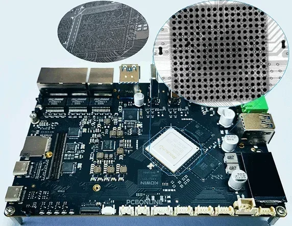
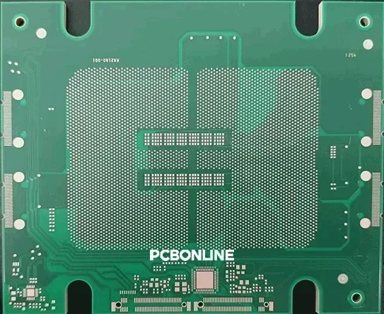
For example, as shown in the above picture, this is the RK3588 control board we produced for our client. The voiding rate of BGA is less than 3%. The breakthrough of this technology demonstrates our advanced BGA soldering capability, the precision of the equipment, and our engineers' experience.
We minimize voiding in BGA soldering through:
- Optimized SMT stencil design with proper aperture ratios.
- Controlled reflow profile with soak stages to allow gas release.
- Strictly controlling the ramp-up and ramp-down rate to prevent thermal shock, warpage, and voiding.
- Proper flux selection to minimize outgassing during reflow, such as lead-free solder SAC305.
Preventing Warpage in BGA Soldering
BGA packages, especially large and thin ones like GPUs, are prone to warpage during reflow soldering. Warpage can cause head-in-pillow defects, bridging, or opens.
To prevent warpage in BGA soldering, we take care of reflow temperature control, BGA storage, baking, verification, and PCB design.
- Reflow profile: We program the oven according to the reflow profile we designed specifically for the BGA PCB. Preheat at 1–2 °C/s, maintain Time Above Liquidus for 30–60 s, set peak temperature according to solder paste specifications, and keep cooling rate below 4 °C/s (follow solder paste and BGA manufacturer's guidelines).
- BGA storage: Keep new BGAs in dry-pack packaging, with desiccant and humidity indicator cards, and ensure they are within the floor life.
- Baking MSL (Moisture Sensitivity Level) 3–5 BGAs: If BGAs are opened or have exceeded their floor life, we bake them according to J-STD-033 or manufacturer recommendations before reflow, usually 125°C (Thicker BGAs (>1.0 mm) for 8–12 hours, and thinner BGAs (≤0.8 mm) for 4–6 hours.).
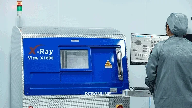
- BGA validation: Before we store the BGAs, we have an X-ray inspection to ensure they are good. After BGA soldering, we also check the BGA solder joints and warpage with a 100% X-ray inspection.
- BGA PCB design check: In our design for manufacturing (DFM), our experienced engineers will optimize the BGA pad, PCB thickness, and heat source distribution if needed, and design the SMT stencil properly.
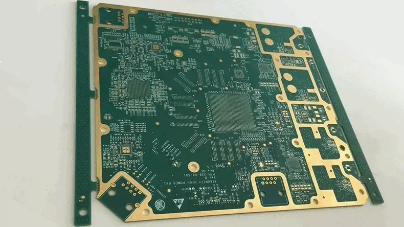
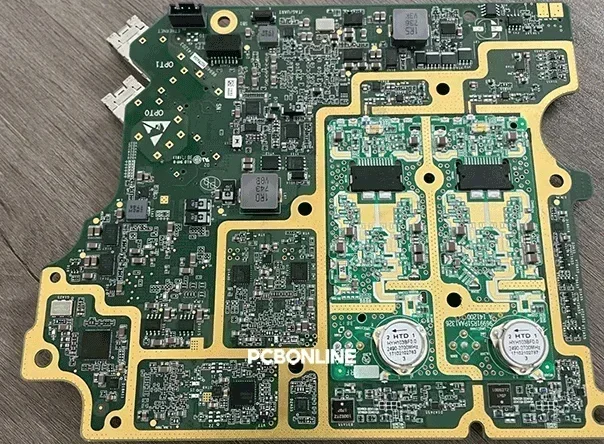
GPU BGA PCB manufactured by PCBONLINE
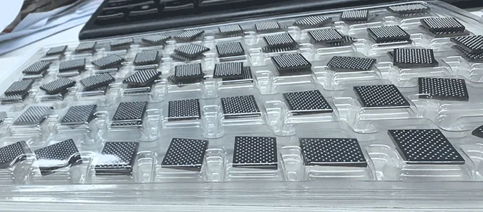
BGA Reballing for Refurbished Chips Before BGA Soldering
BGA reballing is removing old solder balls from a BGA package and replacing them with new ones. If your PCB uses refurbished GPUs (after all, the original new ones are expensive), we can complete the reballing process for you. Its process includes:
- Removing residual solder by reflow and wicking.
- Applying flux and aligning a ball placement machine.
- Attaching new solder balls (typically 0.25–0.5 mm in diameter).
- Reflowing under precise profiles to form reliable solder joints.
- X-ray inspection to ensure ball alignment and joint integrity.
At PCBONLINE, we provide professional BGA reballing and baking for refurbished BGAs before BGA soldering, ensuring they can be reliably assembled.
Inspection and Quality Control in BGA Soldering
Since BGA joints are hidden under the package, automated optical inspection (AOI) is insufficient.
Before BGA soldering, we already check the BGA with X-ray.
If you need IC burn-in programming, PCBONLINE can support transferring your program into the BGA in the Cloud method, which is fully manipulated by you and protects your intellectual properties. During burning in, we can also verify your BGA is in good condition throughout the smooth process.
After BGA soldering, we have a 100% X-ray inspection following IPC-A-610 Class standards to guarantee the highest reliability.
Choose PCBONLINE for BGA PCB Manufacturing and Assembly
At PCBONLINE, we offer more than BGA soldering, as we are a one-stop PCBA manufacturer for advanced electronics manufacturing.
Founded in 2005, PBONLINE has two large advanced PCB manufacturing bases and one PCB assembly factory.
Turnkey BGA PCBA services with SMT and through-hole assembly with 100% X-ray inspection and first-article inspection, including BGA reballing services for refurbished BGAs.
BGA soldering voiding control standard < 5% and can even go down to <3%, exceeding industry standards.
Provide BGA baking and burn-in programming for free if each BGA programming takes less than 30 seconds.
Our professional engineers design the SMT stencil properly for BGA soldering and have rich experience in reflow and wave oven temperature control to reduce the risk of BGA soldering issues like warpage and excessive voiding.
Strict BGA PCBA quality standards with ISO 9001:2015, ISO 14001:2015, UATF 16949: 2016, IPC-A-610 Class 3, RoHS, REACH, and UL certifications.
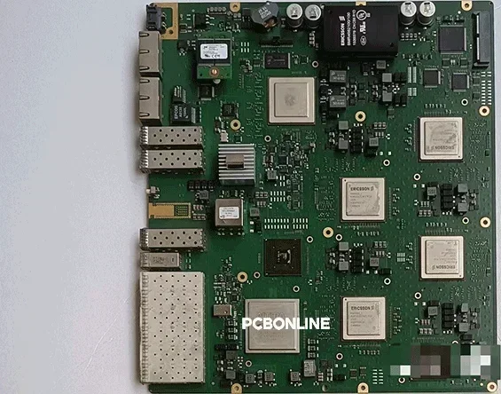
Whether you are designing a GPU server PCB, an AI accelerator module, a networking device, or so on, PCBONLINE has the expertise and capability to deliver reliable BGA PCB assembly at scale. If you feel interested in BGA PCB and soldering from PCBONLINE, send your inquiry by email to info@pcbonline.com.
Conclusion
From ultra-fine pitch 0.35 mm assemblies to voiding control below 5% and GPU reballing services, the challenges in BGA soldering are many. You can have all of them solved by PCBONLINE, providing advanced capabilities and full-service manufacturing.
PCB assembly at PCBONLINE.pdf


