
Ball grid array (BGA) components are ICs with solder balls at the bottom to connect the printed circuit board (PCB). Mounting BGAs on a PCB can be difficult. However, we give you BGA PCB assembly tips in this article to ensure success. You can also read about what a BGA is on PCB, BGA PCB design, and BGA PCB assembly one-stop-shop solution.
Part 1: What is BGA in PCB
![]()
BGA (Ball Grid Array) is an IC package technology that places the solder balls in a grid array at the bottom of the integrated circuit chip. The solder balls are arranged in a grid shape and are connected to the bottom of the chip package. The solder balls function as and better than pins to connect the chip and the PCB. In the BGA PCB assembly process, the balls melt and solder the chip with the circuit board.
BGA is a common packaging method for FPGA chips. The BGA package has high density and reliability. It can provide more functional input and output pins, and the BGA package also has good thermal performance and can be used in high-power applications.
![]()
When you compare a BGA with a dual in-line package (DIP) and a quad flat package (QFP), you can find that the solder balls are much more than the pins of DIP and QFP. Plus a solder ball has a larger contact surface with the PCB than a pin, and a BGA has a much better thermal dissipation capability than a DIP and QFP.
A BGA PCB features:
High-density -
A BGA has thousands of solder balls, and a BGA PCB is a high-density interconnected (HDI) PCB. Plating through holes (PTH) can't be used to connect the BGA to the PCB layers because there are so many pads corresponding to the BGA, and the distance between the pads is small. Usually, a BGA PCB requires blind and buried holes to wire the BGA and the PCB.
High thermal-conductivity
A BGA plays more functions and thus requires more thermal dissipation of the PCB. Thermal transfers from the BGA solder balls to the circuit layers, next to the PCB core, then to the mechanical box and the air.
Besides, you would need close thermal expansion coefficients (CTE) of the BGA and PCB substrate. For example, AlN has a close CTE to semiconductors (IC), and AlN PCB is considered a good option for BGA PCB.
![]()
Types of BGA
We can classify BGAs according to their different packaging materials.
- PBGA uses plastic as the packaging material.
- CBGA uses ceramic as the packaging material.
- TEPBGA uses thermal-enhanced plastic packaging material.
Part 2: BGA PCB Assembly
BGAs are surface-mounted on the PCB like other SMDs. However, during the PCB assembly process, the solder paste inspection machine and automatic optical inspection machine can't inspect the solder balls of the BGA. Their PCB pads are so small and dense. It is easy to cause BGA PCB assembly flaws, such as solder bubbles, cold solder, non-wetting, and de-wetting.
During the SMT manufacturing process, after the solder paste hot-melting and solidifies on the BGA pad, it will cause a certain proportion of bubbles. Bubbles can reduce the mechanical strength of the solder joints, increase the possibility of short circuits, and may affect electrical connections.
According to IPC standards, any solder ball voids larger than 25% of the BGA pad inspection area are considered defects. It should be noted that when the bubble rate is more than 10%, it may affect the reliability and performance of the entire component.
The BGA PCB manufacturerPCBONLINE's BGA welding quality control standard is to control the bubble rate below 5% to ensure welding quality and final product performance.
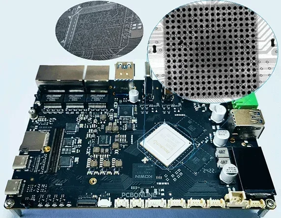
As shown in the picture below, it is an RK3588 control board we produced for our customer. The bubble rate of BGA is less than 3%. The breakthrough of this technology tests the production capability, the precision of the equipment, and the engineers' experience.
How to ensure the success of BGA PCB assembly?
As an experienced PCB assembler, PCBONLINE designs SMT stencils for BGA PCB assembly in a special way.
For the solder paste openings of BGA, we do not design them to match the PCB pads but make them square tin-leak holes that are a little bit larger than the PCB pads.
In this way, enough solder can print onto the PCB pads of the BGA.
Moreover, we have an X-ray inspection before reflow soldering to ensure the solder balls are adequate for soldering the BGA PCB.
The BGA PCB assembly process is in the following steps.
- The solder paste goes through the openings of the PCB stencil and "prints" on PCB pads. The solder paste inspection (SPI) machine scans the PCB mounting-side surface to make sure the solder paste thickness, shape, and size are qualified.
- The surface mount machines pick and place SMDs, including BGAs, on the PCB pads.
- The X-ray machine inspects the solder balls of the BGAs to make sure the position, quantity, size, and shape of the balls are qualified.
- The reflow oven preheats, heats, and cools down the PCB assemblies so that the solder paste and solder balls melt and cure. The alloy powders form the solder joints that tightly connect the components to the PCB.
- Lastly, the automatic optical inspection machine (AOI) scans the PCBA surface to make sure there are no significant issues.
- If the PCB is double-sided, the PCBA will return to the SMT line to mount the other side.
Why does BGA PCB assembly require X-ray inspection? Both the SPI and AOI machines use infrared cameras to scan only the PCBA surface. Due to the array of solder balls at the bottom of the BGA, they are invisible to the SPI machine. But before reflow, the BGAs have to be inspected to avoid possible economic losses.
Only an X-ray machine can inspect the BGAs. The x-ray hits the BGA bottom, showing the solder balls so that we can compare them with the reference to ensure they are qualified for reflow soldering.
If you need BGA PCB manufacturing and assembly, work with the one-stop manufacturer PCBONLINE from the developing phase to bulk production. PCBONLINE will provide you with:
- One-on-one BGA PCB design and engineering support throughout your project.
- BGA PCB manufacturing and assembly from prototypes to bulk production.
- Free IC programming. If your order is equal to or more than $5000, you can enjoy a free complete PCBA sample and functional testing.
- One-stop services, including component sourcing, conformal coating, IC programming, functional testing, thermal aging testing, and box-built.
- Our CAM engineer with more than 20 years of experience can help reduce your manufacturing cost with the optimum BGA PCB design.
Founded in 1999 with two large advanced PCB manufacturing bases and a PCB assembly factory, the BGA PCB/PCBA fabrication is certified with ISO 9001:2015, IATF 16949, IPC, REACH, RoHS, and UL. You can email info@pcbonline.com to get a complex PCB quote.
Part 3: BGA PCB Design
BGA PCB design usually includes:
- Based on the solder ball quantity of the BGA, determine the PCB layer and design the stack up.
- Place the BGA in the center and then smaller components around on the component-mounting side.
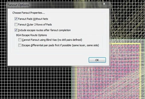
- Fanout the BGA first (fanout means routing from the pad to the PCB layer through PCB holes ) and then other components.
Wiring and fanout happen based on rules you set up, including routing width rules, fanout control rules, routing via style rules, routing layers rules, and electrical clearance rules.
In the PCB design, you can notice that the wires corresponding to different PCB layers have different colors.
![]()
When you design the BGA PCB, you should also consider your PCB supplier's manufacturing capabilities, especially hole drilling.
You can refer to the PCB manufacturer PCBONLINE's drilling and wiring capabilities below.
- Minimum laser drill aperture: 0.075mm (3mil)
- HDI stack up: 1+N+1, 2+N+2, 3+N+3, 4+N+4
- Minimum mechanical drilling aperture: 0.1mm (4mil)
- Minimum PTH pad diameter: 0.3mm
- Minimum trace width/space: 0.035mm/0.035mm
- Resistance control: ±5%
- PCB layers: 2 to 64 layers
Conclusion
BGAs use the solder balls in a grid array to replace the pins so that they have a higher circuit density and better thermal dissipation. BGA PCBs are advanced PCBs used for middle and high-end applications, and you can always believe in the design ability and fabrication quality of one-stop BGA PCB manufacturer PCBONLNIE.
©This article is an original work of the PCBONLINE team. Please indicate the author PCBONLINE if you reprint. If the article is reproduced without permission or indicating the author's source, PCBONLINE reserves the right to investigate the infringement.


