
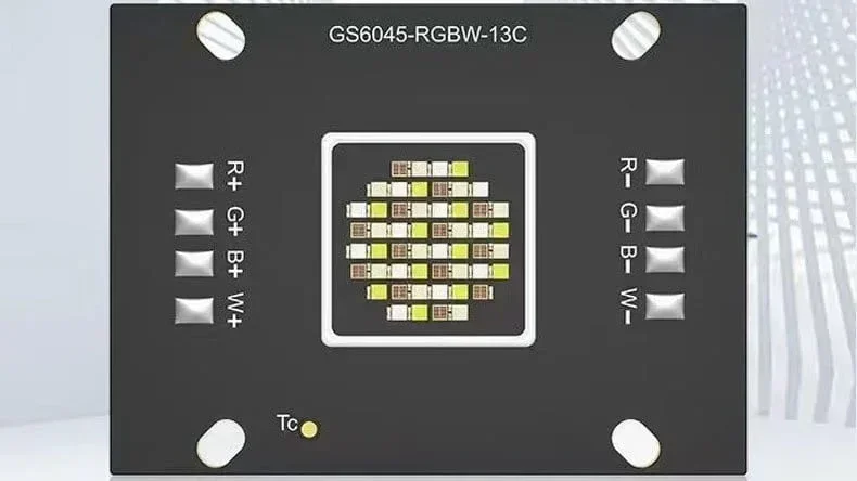
A black PCB uses black solder mask ink and is usually considered high-end. Solder mask colors don't mean their reliability level, but it is almost a custom. For example, Apple was one of the major companies to use black PCBs across their products, leaving an impression that black PCBs are used for "expensive, precision-engineered tech".
Many high-end computer motherboards, GPU PCBs, and automotive-grade PCBs, are black PCB boards due to aesthetic, functional, and marketing factors.
Black Solder Mask Applying
A solder mask is a protective coating that is silkscreen printed or electrostatic sprayed, and then UV-cured and baked to solidify on the surface of the PCB. The PCB ink or oil determines the color of the PCB solder mask. PCB solder mask protects the internal PCB circuits against oxidation, dust, moisture, chemicals, temperature changes, etc.
Liquid photoimageable solder masks are applied on the PCB by the traditional silkscreen printing method. High-density circuits with micro components and thick-copper PCB manufacturing processes adopt the electrostatic spraying technology to apply solder masks.
Silk-screen printing
Silkscreen printing solder masks involves physically pressing the ink through a mesh.
- Pre-treatment: The PCB is cleaned by mechanical scrubbing to remove oils, dust, and oxidation to ensure the ink adheres properly.
- Screen alignment: A fine-mesh stainless steel is aligned over the PCB. Areas that should not be coated, such as holes or pads, are blocked out on the screen.
- Ink application: A squeegee moves across the screen, forcing the liquid solder mask ink through the open mesh and onto the PCB surface.
- Pre-bake: The PCB is placed in an oven to partially cure the ink. This makes it dry to the touch but still chemically reactive for the next stage.
- Imaging and developing: A film containing the circuit pattern is placed over the PCB and exposed to UV light. The light hardens the mask where it's needed. The PCB is then washed in a developer solution to remove the unhardened ink from the pads.
- Final curing: The PCB undergoes a final thermal bake to permanently harden the solder mask.
Electrostatic spraying
Thick-copper PCBs require high-volume PCB ink, while HDI PCBs require high-precision solder mask application. Their PCB fabrication process requires solder mask electrostatic spraying.
- Atomization: The PCB ink is converted into a fine mist using a spray nozzle.
- Electrostatic charging: As the ink particles exit the nozzle, they are given a high-voltage negative electrical charge.
- Attraction: Ground the PCB. Because opposite charges attract, the ink particles are pulled toward the PCB. This "wrap-around" effect. It ensures that even the vertical edges of copper traces and the insides of holes are coated evenly.
- Flash-off: The PCB sits for a short period to allow solvents in the ink to evaporate before baking.
- Curing and developing: Just like the silk-screened boards, the sprayed board is tack-dried, exposed to UV light through a pattern, developed to clear the pads, and finally oven-cured.
How do I choose the right black PCB for my project and what surface finishes are common?
Black solder mask can be matte or glossy. It depends on your aesthetic needs. The color of the solder mask doesn't affect the performance of the PCB.
Green is the most common PCB solder mask color because it is the first color. Black, white, blue, and red are also common PCB colors following green. Other colors are rare.
Though PCB solder mask colors don't change the PCB performance, it affects the visual effect of the legend or silkscreen.
For recognizing the PCB legend easily, such as the symbols and characters, the solder mask and silkscreen should have sufficient color contrast.
Black PCBs usually use white silkscreen. Green PCBs usually use black or white silkscreen. White PCBs usually use black silk screen. Red PCBs usually use white silkscreen. Blue PCBs usually use white silk screen.
Regarding the surface finish for black PCB, it is most common to use ENIG, which is also known as immersion gold. ENIG is the most common surface finish because almost all mid and high-end PCBs can use it. It provides premium solderability, conductivity, and anti-oxidation. Besides, the other common surface finishes for black PCBs include OSP and lead-free HASL.
Where can I buy black PCB boards and what should I look for in suppliers?
Since you are looking for black PCB suppliers, the black PCB you need is not ready-made for DIY, which is a fixed design, but requires custom PCB fabrication.
If your PCB is a standard PCB prototype, which is usually green, you can buy it easily by uploading your Gerber to the cheap prototype PCB manufacturers like JLCPCB and PCBWay, and order online easily.
However, your black PCB is for mid and high-end applications, which require precision and high reliability. You can buy black PCB boards from advanced PCB manufacturers like PCBONLINE. PCBONLINE provides one-stop PCB fabrication and assembly from prototype to bulk production and final device assembly.
What to look for in a PCB supplier is their manufacturing capabilities, engineering experience, technical support, manufacturing quality control, certifications, pricing transparency, and lead time.
Below are some of the PCB manufacturing capabilities of PCBONLINE:
|
Technical Capabilities
|
Plated Through-Hole PCB
|
|
|
Maximum Layers
|
24
|
24
|
|
HDI Stackup
|
3+N+3
|
/
|
|
Max. Processing Board Size
|
24.5" × 28.5" (620 × 720mm)
|
24.5" × 37.5" (620mm × 950mm)
|
|
Min. Line Width/Line Space
|
I/L: 2.5mil/2.5mil O/L: 4mil/4mil (POFV)
|
I/L: 2.5mil/2.5mil O/L: 4mil/4mil(POFV)
|
|
Board Thickness
|
3.5mm
|
4.0mm
|
|
Min. Drill Bit
|
6mil
|
6mil
|
|
Aspect Ratio
|
18:01
|
18:01
|
|
Min. Micro Via & Aspect Ratio
|
4mil & 0.8:1
|
/
|
|
Min Core Board Thickness
|
2mil
|
2mil
|
|
Alignment between Layers
|
5mil
|
5mil
|
|
Solder Mask Tolerance
|
±8%
|
±8%
|
|
Back Drill stub
|
2-10mil
|
2-10mil
|
|
Copper Fill
|
Yes
|
/
|
|
POFV
|
Yes
|
Yes
|
|
Skip-via (L1-3)
|
No
|
No
|
|
Buried Copper Block
|
Yes
|
Yes
|
|
Buried Capacitance
|
No
|
No
|
|
Technical Specifications
|
Flexible PCB Capabilities
|
|
Layer Count
|
1-8L
1-4 L (normal) |
|
PCB thickness
|
0.1-0.5mm (1-4L)
0.6-0.8mm (5-8L) |
|
The tolerance of flex PCB thickness (≤0.3mm) (exclude stiffener)
|
±0.03mm
|
|
The tolerance of multilayer flex PCB thickness (≤0.3mm-0.8mm) (exclude stiffener)
|
±10%
|
|
The tolerance of flex PCB thickness (include PI/FR4 stiffener)
|
±10%
|
|
Maximum finished flex PCB size
|
7.8inch*21.8inch(PI≥1mil)
7.8inch*14inch (normal) |
|
Minimjm finished flex PCB size
|
2mm*4mm (no connection tab)
8mm*8mm (with connection tab) |
|
Minimum Line Width/Line Space
|
0.035mm/0.035mm
|
|
Min. Interlayer Alignment
|
±0.05mm
|
|
Min. Hard Board Dielectric Layer Thickness
|
/
|
|
Surface Finishes
|
ENIG, OSP, ENEPIG, Immersion Tin
|
|
Applications
|
display module, smartphone, camera module, consumer electronics
|
|
Technical Specifications
|
Rigid-Flex PCB Capabilities
|
|
Maximum Layers
|
24
|
|
Flex Layer Count
|
11-20L (18L)
|
|
Min. Laser Blind Hole Aperture
|
0.1mm
|
|
Flex layer on outer or Middle Layer
|
Middle
|
|
Finished PCB thicknes
|
0.2mm-4.0mm
|
|
Tolerance of PCB thickness
|
>1.0mm, ±10%
≤1.0mm, ±0.1mm |
|
Min flex layer width
|
2.5mm
|
|
Min flex layer width between rigid
|
3mm
2mm(limit) |
|
Maximum PCB panel size
|
406mm*736mm
|
|
Minimum PCB panel size
|
10mm*15mm
|
|
Impedance tolerance
|
Single-ended: ±3Ω(≤50Ω), ±8%(>50Ω)
Differential pair: ±4Ω (≤50Ω), ±8%(>50Ω) |
|
HDI type
|
3+n+3 (n buried hole≤0.4mm)
|
|
Minimum twist & warpage
|
0.75%(symmetrical
1.5%(asymmetrical) |
|
Adhesive dispense width
|
1.5±0.5mm (slot width≥5mm)
|
|
Min distance between R-F connect area to conductor
|
0.3mm(half depth slot process)
0.5mm normal |
|
Min. width of resin flow out in R-F connect area
|
0.5mm
1.0mm normal |
|
Min distance between E-test pads
|
3mil
4mil normal |
|
Min BGA pad size BGA
|
10mil (electrical Ni/Au7mil)
12mil (electrical Ni/Au8mil) normal |
Order Black PCB from PCBONLINE
Founded in 2005, PCBONLINE has more than 20 years of experience in PCB manufacturing and assembly, and finished device OEM manufacturing. We provide one-on-one engineering support for every project, no matter what quantity of PCB/PCBA/devices you want.
Types of Black PCBs Offered at PCBONLINE
PCBONLINE offers multiple types of black PCBs.
|
Type
|
Layer count range
|
Key materials/substrates
|
Applications/advantages
|
|
FR4 PCB
|
1 to 64 layers
|
Standard FR4, High-TG FR4 material for thermal stability
|
General electronics, computers, communications, power distribution, and large-volume PCBs where cost vs performance balance matters.
|
|
HDI PCB
|
4 to 64 layers with microvias / laser drilled
|
FR4 substrate, fine copper foils, laser drilling
|
Mobile devices, compact electronics, RF / high speed, and aerospace, where routing density and signal integrity are critical.
|
|
Rigid-flex PCB
|
2 to 24 layers
|
FR4 and polyimide substrate
|
Space-constrained designs, aerospace, military, medical implants, devices with moving hinges or folding parts.
|
|
High-frequency PCB
|
4 to 24 layers
|
PTFE, Rogers, ceramics, specially formulated FR4 / laminates, or Rogers/FR4 hybrid laminates, good dielectric constant control, strict impedance control.
|
High-speed digital, RF, and microwave systems, antennas, and high-frequency communication gear.
|
|
Aluminum and copper-core PCB
|
Aluminum PCB: 1 to 4 layers
Copper-core PCB: 1 to 8 layers |
Aluminum, copper / excellent thermal conductivity and power distribution.
|
Automotive, LED lights, industrial controls.
|
If you need one-stop black PCB manufacturing from prototyping to mass production, you can partner with PCBONLINE.
PCBONLINE has strong PCB manufacturing capabilities, including FR4 PCB layers from 1 to 64, high-density PCB, high-frequency PCBs, flexible PCB, rigid-flex PCB, aluminum PCB, copper-based PCB, and ceramic PCB.
PCBONLINE offers free design for manufacturing (DFM) for your PCB and PCBA project, including checking Gerber, bill of materials (BOM), testing files, and solving all technical and unexpected issues during prototyping to ensure the smooth and successful massive production.
PCBONLINE can do the R&D for your PCBA project or take part in your project's development from the early stage for the optimum PCB design and prevent tricky problems in the field application engineering (FAE) stage.
One-stop PCB services meeting your custom needs, including prototyping/sampling, PCB manufacturing, component sourcing, PCB assembly, PCBA value-added, enclosure, and box-build assembly.
High-quality advanced PCB manufacturing certified with ISO 9001:2015, ISO 14001:2015, IATF 16949:2016, RoHS, REACH, UL, and IPC-A-600 Class 2/3.
No matter what applications of your black PCB are, like automotive, aerospace, medical devices, IoT, and high-end consumer electronics, PCBONLINE can produce and assemble PCBs that meet the highest performance and reliability standards. To get a quote for your PCB project, contact info@pcbonline.com.
Conclusion
PCB solder mask colors don't affect PCB performance, but your PCB design should ensure sufficient color contrast between the solder mask and silkscreen. Black PCBs use white silkscreen to recognize the symbols and marks. It is a custom to use black PCBs for high-end applications. If you're looking for a black PCB supplier, PCBONLINE can provide one-stop manufacturing and one-on-one engineering support for you.
PCB assembly at PCBONLINE.pdf
PCB fabrication at PCBONLINE.pdf


