
The artificial intelligence (AI) boom is entering its second major phase. For the past few years, the tech world has focused heavily on AI training clusters. Building large language models (LLMs) required massive, centralized data centers packed with ultra-high-performance servers.
Today, the focus is rapidly shifting from training to AI inference. Inference is the phase where trained AI models process live data to answer real-time AI prompts.
The AI transition from training to inference is changing the physical foundation of technology. It is triggering a massive overhaul in AI hardware infrastructure, specifically within the Printed Circuit Board (PCB) market. After 90 years of acting as a low-margin component, the humble PCB is suddenly the most critical bottleneck and growth driver in AI hardware.
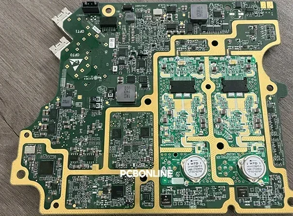
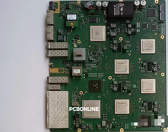
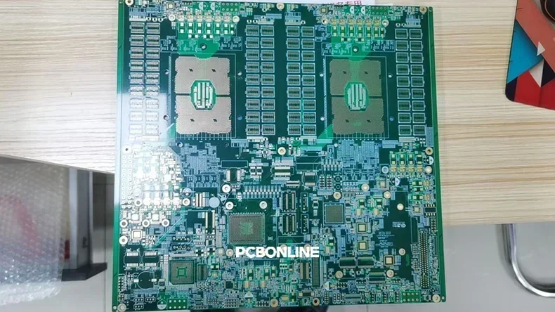
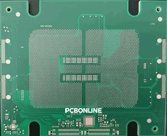
HDI 24+ layers: To support ultra-high-density routing of PCIe Gen5, NVLink, and high-bandwidth memory interfaces, AI server PCBs are typically 24 layers or more.
Power delivery for high wattage: Each GPU consumes hundreds of watts. Wide copper planes and advanced VRM design are required for stable operation.
Thermal management: Thick copper, thermal vias, and optimized stack-ups are used to manage massive heat output.
Signal integrity: Inner-layer high-speed traces reduce crosstalk and electromagnetic interference (EMI).
AI server PCBs are the most advanced printed circuit boards in the PCB industry. They align with PCBONLINE's mid-to-high-end PCB manufacturing positioning.
AI Infrastructure: From Centralized Training to Distributed Inference
To understand why AI infrastructure is changing, we have to look at how data moves: [AI training era] --> Centralized clusters --> Few, massive server farms [AI inference era] --> Distributed network --> Edge servers, private data centers, AI devices.
During the training era, tech giants needed a small number of centralized supercomputers. These facilities housed thousands of interconnected GPUs working on a single problem.
The inference era is completely different:
When millions of users type AI prompts into applications simultaneously, they expect instant answers. Sending every single query back to a central supercomputer in California or Virginia creates massive latency (delay).
To solve this issue, AI infrastructure architecture must become distributed.
Inference requires computing power to live closer to the user. This means deploying AI servers at:
- The city edge: Localized data centers in major metropolitan areas.
- Enterprise private server rooms: On-premise infrastructure for corporate data security.
- AI devices: On-device chips in laptops, smartphones, and robotics.
Instead of a few thousand specialized servers in a handful of locations, the world now needs millions of inference-ready servers spread globally. This massive footprint is driving an exponential surge in hardware demand.
How Nvidia Reshaped the Hardware Landscape
NVIDIA is the undisputed leader in AI infrastructure components. The company does not just design faster chips; it completely reimagines how server components communicate.
In older server designs, PCBs were seen as simple "highways" to connect electronic components. They were lightweight, relatively cheap to make, and cost thousands of dollars per server rack.
NVIDIA changed the rules by using high-end PCBs as the actual computational foundation for Artificial General Intelligence (AGI). As data transfer speeds between GPUs climbed, traditional copper wires and low-grade boards failed. They caused signal loss and overheated.
The GB200 Cabinet Revolution
With the introduction of the Nvidia GB200 NVL72 architecture, Nvidia made a radical design choice. They moved the internal connections of the server cabinet away from heavy cabling and brought them right back onto the PCB.
This architectural pivot had an immediate impact on the value of the components:
- Value multiplier: The value of the PCB inside a single GB200 server cabinet jumped by 4 to 6 times compared to previous generations.
- Cost scaling: At the macro level, data center spending on advanced PCBs has scaled from millions of dollars across the industry to billions of dollars globally.
The Triple Upgrade: Inside High-Speed Advanced PCBs
To handle high-volume processing from millions of concurrent AI prompts, standard PCBs are no longer sufficient. The industry is currently experiencing a "Triple Upgrade" across material science, structural architecture, and manufacturing precision.
1. Material Evolution: From FR4 to M8 Resin
For decades, FR4 (Flame Retardant 4) was the gold standard material for circuit boards. It is cheap, reliable, and easy to manufacture. However, at high frequencies, FR4 absorbs too much signal energy.
AI infrastructure demands a shift to High-Velocity PCBs (HVPCBs). The industry is moving away from FR4 to ultra-low-loss materials like M8-grade resins. These advanced polymers keep signal degradation to an absolute minimum, ensuring data moves at maximum speed across the board.
2. Structural Architecture: Skyrocketing Layer Counts
A standard computer or server board usually features 10 to 16 layers of circuitry squeezed together.
AI inference clusters handle immense parallel workloads. To route all these data pathways without cross-talk or interference, the layer count on advanced AI boards has jumped to 30 to 40 layers. Manufacturing a stable, flat board with 40 perfectly aligned layers is an incredible feat of engineering.
3. Manufacturing Process: Nano-Scale HDI Laser Drilling
When you pack 40 layers of circuitry into a tight space, you can no longer use mechanical drill bits to create electrical connections between layers.
Manufacturers now utilize High-Density Interconnect (HDI) technology. This process uses ultra-precise lasers to drill microscopic holes (microvias) at a nanometer scale. An HDI PCB allows for incredibly dense component placement and shorter routing paths, which cuts down latency.
|
Technical metric
|
Technical metric interval
|
Advanced AI inference PCBcinterval
|
|
Core material
|
Core material
|
M8-grade resin / ultra-low-loss polymers
|
|
Layer count
|
Layer count
|
30 to 40 layers
|
|
Drilling tech
|
Mechanical drilling
|
Mechanical drilling
|
|
Relative value
|
Relative value
|
Relative value
|
The Great Industry Reshuffle
The PCB industry is 90 years old. For a long time, it was criticized for being a low-margin, highly cyclical commodity business. It was an industry where companies cut prices to the bone just to win high-volume orders.
The AI inference revolution has permanently broken that cycle.
We are now witnessing a deep market reshuffle. The industry is splitting into two distinct tiers:
The commodity tier: Low-end manufacturers stuck making cheap, low-layer boards for legacy electronics. These companies face shrinking margins and fierce price wars.
The advanced AI tier: A select group of high-tech manufacturers capable of producing 40-layer, M8-resin, HDI laser-drilled boards.
The barrier to entry for the advanced tier is incredibly high. It requires billions of dollars in new capital expenditures for laser machinery, clean rooms, and advanced chemistry labs.
As a result, the companies that master this supply chain are securing massive, high-margin contracts with AI hyperscalers.
Partner with PCBONLINE for Turnkey AI Server PCBs
If you are designing next-generation GPUs for AI and GPU servers, work with PCBONLINE for turnkey OEM service. We provide AI server PCB manufacturing services that cover GPU PCB manufacturing, assembly, testing, and reliability assurance.

Founded in 2005, PBONLINE has two large advanced PCB manufacturing bases and one PCB assembly factory.
AI server PCB fabrication with HDI via-in-pad copper filling for GPU designs with 24+ layers.
We provide one-stop AI server PCB manufacturing, including component sourcing, PCB fabrication, assembly, testing, and system integration.
SMT assembly with fine-pitch BGA placement accuracy and custom reflow profiles for warpage-free soldering.
100% X-Ray inspection, functional testing, and burn-in testing for guaranteed reliability.
We have rich experience in impedance control, oven temperature control, and assembly fixture designs.
Supporting IC programming in the Cloud way, manipulated by you, and protecting your intellectual property.
High-quality PCBA manufacturing certified with ISO 9001:2015, ISO 14001:2015, IATF 16949:2016, RoHS, REACH, UL, and IPC-A-610 Class 2/3.
At PCBONLINE, we can help our clients reduce costs while achieving the highest levels of performance and reliability. If you feel interested in AI server PCBs from PCBONLINE, send your inquiry by email to info@pcbonline.com.
FAQ: Understanding AI Infrastructure and PCB Upgrades
Q1: What is AI infrastructure?
AI infrastructure refers to the physical hardware and underlying stack required to train and run AI models. This includes specialized GPUs, high-speed networking, advanced storage systems, cooling facilities, and high-performance Printed Circuit Boards (PCBs).
Q2: Why do AI prompts require better hardware infrastructure?
When an end-user inputs an AI prompt, the system must generate a response instantly using an active model (inference). Processing thousands of prompts simultaneously requires massive data bandwidth, low latency, and zero signal loss across the server components.
Q3: What is the difference between FR4 and HVPCB?
FR4 is a standard, cost-effective fiberglass material used in everyday electronics. High-Velocity PCBs (HVPCBs) use advanced resins (like M8) designed to handle ultra-high frequencies and rapid data transfer speeds without overheating or losing signal integrity.
Q4: Why did Nvidia increase the use of PCBs in the GB200?
NVIDIA integrated connections directly back onto the PCB in the GB200 architecture to eliminate the physical limitations, clutter, and signal degradation associated with traditional internal cabling. This change dramatically improves data speeds within the cabinet but requires highly advanced, multi-layer PCBs.
Conclusion
Neural network architectures, and clever AI prompts cannot run without hardware. The physical reality of the AI inference era is a massive, distributed web of hardware. Every single edge server, enterprise data room, and smart device requires a highly customized, ultra-high-speed PCB to handle the data load. As the global demand for AI computing grows, China supplies over 70% of AI server PCBs, with PCBONLINE standing out as a reliable turnkey AI server PCB manufacturer. If you are looking for a trusted partner for AI server PCBs, contact PCBONLINE for turnkey OEM manufacturing.
PCB assembly at PCBONLINE.pdf


