
Welding circuit boards is a core process in electronics manufacturing and prototype development, directly determining the reliability, performance, and long-term stability of electronic products. For electronics engineers, hardware developers, and maintenance technicians, mastering precise and reliable welding techniques is not only a fundamental skill but also a critical factor in ensuring the functional integrity of circuit boards. This article will delve into three core technical dimensions of welding circuit boards: Welding Principles and Materials Science, Precision Welding Process Flow, and Welding Defect Analysis and Reliability Enhancement. Through a systematic analysis of the physical and chemical mechanisms, practical process techniques, and solutions to common issues in welding, this guide aims to provide engineers with a comprehensive and professional technical manual for welding circuit boards.
In this article:
Part 1. Materials Science and Physicochemical Principles of Welding Circuit Boards Part 2. Precision Welding Process Technology and Flow Control Part 3. Root Cause Analysis of Welding Defects and Strategies for Reliability EnhancementMaterials Science and Physicochemical Principles of Welding Circuit Boards
Metallurgical Fundamentals and Selection Criteria for Solder Alloys
The essence of welding is forming a metallurgical bond between the base metal (typically a copper pad) and a molten metal alloy, creating a reliable electrical connection and mechanical fixation. The most commonly used solder alloys are tin-based. While tin-lead (Sn-Pb) alloys historically dominated, lead-free solders (e.g., SAC305: 96.5% Sn, 3% Ag, 0.5% Cu) have become the industry standard due to environmental regulations.
Key Metallurgical Characteristics:
- Eutectic Point and Melting Point: Eutectic alloys have the lowest melting point, e.g., Sn63/Pb37 eutectic at 183°C. Lead-free solders like SAC305 melt at 217-220°C, imposing stricter requirements on the temperature profile.
- Wettability: Refers to the ability of molten solder to spread on a copper surface, dependent on surface tension, flux activity, and substrate metal cleanliness. Good wetting forms a concave meniscus with a contact angle less than 90°.
- Intermetallic Compound (IMC) Formation: During welding, tin reacts with copper to form Cu6Sn5 (η-phase) and Cu3Sn (ε-phase). A moderate, continuous IMC layer (typically 1-3µm) is crucial for joint strength, but an excessively thick or uneven IMC layer can lead to brittle fracture.
Solder Selection Guidelines:
- High-Reliability Applications: Aerospace and medical equipment recommend silver-containing solders (e.g., SAC305) for superior thermal fatigue resistance and strength.
- Fine-Pitch Components: Choose low surface tension solder pastes, such as bismuth (Bi)-doped alloys, to improve wetting on tiny pads.
- Manual Soldering: Match solder wire diameter (0.5mm-1.0mm) to pad size. Select flux activity level (ROL0, ROL1) based on oxidation level.
Chemical Mechanisms and Performance Optimization of Fluxes
Fluxes remove oxides, reduce surface tension, and prevent re-oxidation during soldering. Their chemical composition directly determines soldering quality and post-process cleaning requirements.
Flux Chemical Composition:
- Activators: Organic acids (e.g., succinic acid, adipic acid) or halides (halogen content <0.2% for halogen-free). Responsible for decomposing metal oxides upon heating.
- Vehicle (Resin): Rosin or resins provide thermal coverage and form a protective film upon cooling.
- Solvents: Ethanol or glycerol control viscosity and evaporation rate.
Choice Between No-Clean and Water-Soluble Fluxes:
- No-Clean Fluxes: Solid content <2%, minimal residue, and low ionic contamination (typically <1.56 µg NaCl/cm²). Suitable for consumer electronics. Note: Hygroscopic residues may cause electromigration in high-voltage environments.
- Water-Soluble Fluxes: Contain higher activator levels. Require post-solder cleaning with deionized water. Can reduce residual ionic contamination to below 0.1 µg NaCl/cm². Suitable for high-reliability military or automotive electronics.
Influence of Substrate Materials and Pad Design on Solderability
The PCB substrate material and pad design are inherent factors determining soldering success rates.
Common Substrate Properties:
- FR-4 Glass Epoxy: Tg (Glass Transition Temperature) between 130-180°C. Multiple reflow cycles (>260°C) may cause delamination or copper foil peeling.
- High-Frequency Laminates (e.g., Rogers RO4003): Low loss factor but different thermal conductivity, requiring adjustment of thermal capacity during soldering.
Key Pad Design Parameters:
- Thermal Balance Design: Use thermal relief pads for large ground pads to prevent excessive heat dissipation leading to poor soldering.
- Pad Size and Spacing: According to IPC-7351 standard, 0402 component pads should be 0.3mm longer than the component end cap. Spacing should ensure fillet formation without bridging.
- Surface Finish Selection:
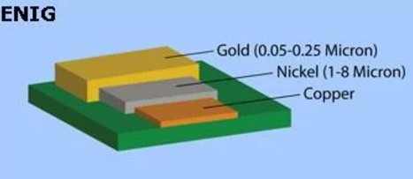
Electroless Nickel Immersion Gold (ENIG): Provides a flat surface suitable for fine-pitch BGAs. Beware of "Black Pad Phenomenon" (phosphorus enrichment causing brittleness).
Organic Solderability Preservative (OSP): Eco-friendly and low-cost, but short shelf life (typically 3-6 months) and unsuitable for multiple reflows.
Immersion Silver: Excellent solderability but prone to sulfidation (tarnishing). Requires moisture-proof sealed storage.
Precision Welding Process Technology and Flow Control
Reflow Soldering Temperature Profile Optimization and Thermal Dynamics Analysis
Reflow soldering is the core process in SMT production. The temperature profile directly determines solder joint quality and component reliability.
Four-Stage Temperature Profile Analysis:
-
Preheat Zone (Ramp-up): Ramp rate of 1-3°C/sec. Too fast causes thermal shock; too slow depletes flux prematurely. Goal: uniformly heat PCB to ~150°C.
-
Soak Zone (or Preheat Zone): Temperature maintained at 150-180°C (150-200°C for lead-free). Duration: 60-120 seconds. This stage equalizes PCB temperature, reduces delta T, volatilizes solvents, and activates flux.
-
Reflow Zone: Peak temperature should be 20-30°C above the solder liquidus temperature. For SAC305, recommended peak is 240-250°C. Time Above Liquidus (TAL) should be 45-90 seconds. Exceeding 250°C or excessively long TAL accelerates IMC growth and substrate damage.
-
Cooling Zone: Ideal cooling rate is 2-4°C/sec. Rapid cooling refines grain structure, improving fatigue resistance, but excessive speed may crack components.

Thermal Dynamics Challenges and Solutions:
- Thermal Balancing for Large BGAs and Small Chip Components: Use zone heating, bottom-side preheating, or thermal shielding fixtures.
- Thermocouple Placement: Monitor at least four points: board edge, board center, high-mass components (e.g., connectors), and thermally sensitive components (e.g., MLCCs).
Selective Soldering and Manual Precision Soldering Techniques
For mixed-technology boards (through-hole and SMT) or rework scenarios, selective and manual soldering are essential skills.
Key Points for Selective Soldering Processes:
- Drag Soldering: Suitable for multi-pin connectors. Control solder wave height to half the board thickness. Drag speed: 3-8 mm/sec, angle: 5-7°.
- Jet Soldering: For localized joints. Nitrogen atmosphere can reduce dross formation by up to 80%.
Manual Precision Soldering Operation Standards:
-
Tool Selection: Match iron tip shape (chisel, knife, conical) to the pad. Temperature control precision ±5°C. For lead-free soldering, use a 70W+ high-frequency soldering iron.
-
Five-Step Soldering Method:
-
Clean the tip on a damp sponge or brass wool.
-
Contact the pad and lead, preheat for 1-2 seconds.
-
Feed solder wire from the opposite side, not directly onto the iron tip.
-
Remove solder wire first, then the iron, after solder flows.
-
Keep components stationary during cooling to avoid movement.
-
- Rework for QFN/LGA (Bottom-Termination Devices): Use specialized hot air nozzles. Preheat the bottom side to 150°C. Hot air temperature: 300-320°C, duration not exceeding 30 seconds.
Welding Quality Inspection and Process Verification Methods
Welding quality must be verified through multi-level inspection techniques.
Non-Destructive Inspection Techniques:
- Automated Optical Inspection (AOI): Inspects solder joint shape, position, and shine. Limited for hidden joints (e.g., BGA).
- Automated X-Ray Inspection (AXI): Detects BGA voiding, bridging, and insufficient solder. Voiding >25% or single void diameter >1/3 of ball diameter is typically rejected.
- Scanning Acoustic Tomography (SAT): Used to detect internal delamination or cracks in encapsulated components.
Destructive Analysis and Process Verification:
- Cross-Sectioning: Polish and etch samples to measure IMC thickness and solder joint grain structure.<
- Solder Ball Shear/Pull Test: According to IPC-9701, shear force for lead-free joints is generally required to be >25g/mil².
- Thermal Cycling Test: -40°C to 125°C, 1000 cycles. Resistance change <20% is acceptable.
Root Cause Analysis of Welding Defects and Strategies for Reliability Enhancement
Diagnosis and Correction of Systemic Welding Defects
Welding defects often result from the interaction of materials, design, and process, requiring systematic analysis.
Common Defects and Root Causes:
|
Defect Type
|
Potential Causes
|
Corrective Actions
|
|
Cold Solder Joint
|
Low temp, vibration, contamination
|
Increase temp, secure cooling, use fresh solder
|
|
Solder Bridging
|
Excess paste, misalignment, large aperture
|
Adjust stencil, improve alignment, optimize pad design
|
|
Tombstoning
|
Uneven heating, paste imbalance, fast ramp
|
Balance thermal design, equalize paste, slow ramp
|
|
Voids
|
Trapped gas, oxidation, flux outgassing
|
Use vacuum reflow, optimize paste, control atmosphere
|
|
Solder Balling
|
Moisture, steep profile, excess flux
|
Dry storage, flatten profile, reduce paste volume
|
Advanced Materials and Technologies for High-Reliability Soldering
Extreme environment applications (high temperature, humidity, vibration) require enhanced soldering solutions.
High-Performance Soldering Materials:
- Nanoparticle-Doped Solders: Adding nano-copper (50-100nm) or nano-nickel particles can refine grains, improving creep resistance by over 30%.
- Electrically Conductive Adhesives (ECAs): Silver-filled epoxy resins, curing temperature <150°C, suitable for heat-sensitive substrates (e.g., flexible circuits).
- Low-Temperature Soldering (LTS) Technology: Bismuth-based alloys (e.g., Sn42Bi58, melt point 138°C) significantly reduce thermal stress but are brittle; adding trace rare-earth elements can improve toughness.
Process Technologies to Enhance Soldering Reliability:
- Pulse-Heating Soldering: Achieves localized rapid heating via microsecond current pulses, minimizing the heat-affected zone. Suitable for micro-assembly.
- Vacuum Reflow Soldering: Reduces chamber pressure to <1 mbar, decreasing voiding to <1%, significantly improving thermal and mechanical performance.
- Laser Soldering: Fiber laser (wavelength 808-980nm) focus diameter can be as small as 50µm with controlled energy density. Suitable for high-density interconnects and thermally sensitive components.
Long-Term Reliability Assessment and Life Prediction of Solder Joints
Solder joint failures in service primarily stem from thermomechanical fatigue, electromigration, and chemical corrosion.
Failure Mechanisms and Accelerated Test Models:
- Thermal Cycling Fatigue: Plastic strain accumulation due to CTE mismatch during temperature cycling. Use the Coffin-Manson relationship for life prediction:
-
Nf=A⋅(Δϵp)−n
- Electromigration: At high current densities (>10^4 A/cm²), electron wind force causes metal ion migration, forming voids or whiskers. Black's equation describes Mean Time To Failure (MTTF): MTTF=A⋅j−nexp(Ea/kT)
where j is current density, E_a ≈ 0.8-1.2 eV.
-
Corrosion Failure: Chloride or sulfide residues cause electrochemical corrosion in humid environments. Use Temperature-Humidity-Bias (THB) testing (e.g., 85°C/85%RH/5V bias, 1000 hours) with acceptance criteria: resistance change <10%.
where Δε_p is the plastic strain range; n ≈ 2-3 for lead-free solder.
Reliability Design Guidelines:
- Strain-Sensitive Components (e.g., Large BGAs): Apply underfill epoxy, which can improve thermal cycle life by 5-10 times.
- High-Current Solder Joints: Increase joint volume, use high-silver-content solder, or replace solder balls with copper pillars.
- Vibration Environments: Apply conformal coating to through-hole components or use connectors with locking mechanisms.
Welding circuit boards is a multidisciplinary technology integrating materials science, thermodynamics, metallurgy, and process engineering. Every aspect—from the microstructure of solder alloys to the macroscopic temperature profile of reflow, from the manual dexterity of soldering to the failure physics analysis of high-reliability products—requires engineers to deeply understand the principles and precisely control parameters. As electronic devices evolve towards miniaturization, high density, and high power, soldering technology will continuously face new challenges, such as ultra-fine-pitch (<0.3mm) interconnects, heterogeneous integration (mixing silicon, glass, metal substrates), and extreme environment adaptability. By mastering the core principles and process methods outlined in this article, combined with continuous practice and data analysis, engineers can establish stable and reliable soldering processes, laying a solid foundation for the performance and longevity of electronic products.
One-Stop HDI PCB Manufacturer and Its PCB Via Filing Capabilities
If you're looking for turnkey HDI electronics manufacturing services (EMS) from hardware development to PCBA fabrication and box-build assembly, you can work with the one-stop HDI PCBA manufacturer PCBONLINE.
Founded in 1999, PCBONLINE has R&D capabilities for HDI projects and EMS manufacturing capabilities, including via filling for stacked vias. It provides 4-to-64-layer HDI PCB fabrication, assembly, and PCBA box-build assembly. You can order various HDI PCBs from PCBONLINE, such as FR4, polyimide (flexible PCB), polyimide + FR4 (rigid-flex PCB), and PTFE/Rogers (high-frequency PCB).

3000m² of production capacity per day for HDI PCBs with builds of 1+N+1, 2+N+2, 3+N+3,4+N+4, and arbitrary interconnection in any layers.
PCBONLINE has hardware and software R&D capabilities for IoT applications requiring HDI design, including PCBA and enclosures.
We can manufacture complex PCBs with stacker vias, via-in-pad, microvias, inlay boards, heavy copper designs, and hybrid and fine structure lay-ups.
Besides HDI PCB fabrication, we have powerful capabilities in fine-pitch assembly for HDI PCB assembly.
We have rich R&D and manufacturing experience for HDI applications such as FPGA boards.
High-quality HDI PCB and PCBA manufacturing certified with ISO 9001:2015, IATF 16949, RoHS, REACH, UL, and IPC-A-610 Class 2/3.
Here'e the PCB via filing capabilities at PCBONLINEL:
- Micriavia filling with copper: laser via size 0.1-0.125mm, priority 0.1mm
- Finished hole size for via-in-pad filling with resin: 0.1-0.9mm (drill size 0.15-1.0mm), 0.3-0.55mm normal (drill size 0.4-0.65mm)
- Max aspect ratio for via-in-pad filling with resin PCB - 12: 1
- Min resin plugged PCB thickness: 0.2mm
- Max via-filling ith resin PCB thickness: 3.2mm
- Making different hole sizes with via filling in one board: Yes
- Via filling with copper/silver: Yes
If you need HDI PCBAs or any other PCBAs requiring via filling, please send your email to PCBONLINE at info@pcbonline.com. We will provide one-on-one engineering support to you.
Conclusion
Via filling is used for creating stacked vias in HDI PCB fabrication, BGA/CSP/QFN IC packaging, and filling PCB via-in-pad with resin during multilayer PCB fabrication. If you need one-stop electronics manufacturing for your HDI PCBA project, contact the one-stop advanced PCB manufacturer PCBONLINE for high-quality PCBA and box-build solutions tailored to your project's needs.
PCB fabrication at PCBONLINE.pdf


