
In AI hardware, selecting high-speed PCBA is akin to building the neural network and circulatory system for a “superbrain.” It directly determines data flow velocity, power stability, and thermal management efficiency. When confronting diverse PCB types—including HDI, high-frequency/high-speed, high-layer count, metal-core substrates, and rigid-flex boards—engineers must deeply comprehend the unique signal integrity, power integrity, and thermal management demands of AI hardware. This article will guide you in identifying the optimal PCBA solution for your AI project from numerous technical options, based on computational requirements, power consumption characteristics, spatial constraints, and budgetary limitations. This ensures your hardware platform can fully unleash its potential.
In this article:
Part 1. Common PCB Types Part 2. Core Technical Challenges in AI Hardware PCBA Part 3. How to Choose the Right PCBACommon PCB Types
Selecting high-speed PCBA (printed circuit board assembly) for AI hardware is akin to designing and constructing the “neural network” and “blood circulation system” for a “superbrain,” requiring meticulous consideration. For AI hardware—whether GPU accelerator cards in servers, dedicated AI training/inference modules, or AI computing units in edge devices—the core objective of PCBA is to ensure high-speed data flow, stable power supply, and efficient thermal management.
The following are common PCB types:
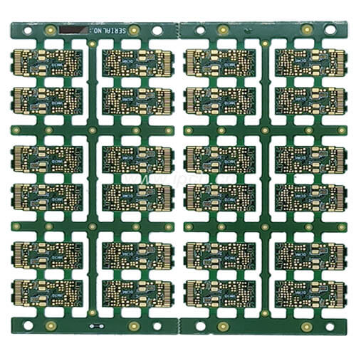
HDI PCBAHDI PCBA is a key technology enabling miniaturization and high-performance integration in AI hardware. Its core lies in utilizing laser-drilled microvias (blind and buried vias), fine traces (line width/spacing down to 50μm), and high-layer designs (typically 8 layers or more). This process enables high-density routing within minimal space, directly accommodating the dense BGA pins of AI chips (such as GPUs/ASICs). It reduces signal path length and parasitic effects, thereby enhancing signal integrity and transmission rates. In AI applications, HDI boards are commonly found in smartphone NPU modules, edge computing devices, and high-end chip packaging substrates, meeting stringent demands for computational density and space efficiency.
High-frequency, high-speed PCBA focuses on resolving signal integrity challenges at GHz-level transmission. Its core lies in utilizing specialized low-loss dielectric materials (such as Megtron 6, Tachyon, or RO4000 series), rigorously controlling impedance (tolerance within ±5%) and minimizing dielectric loss (Df value < 0.005) to reduce signal attenuation. These boards feature stable dielectric constants (Dk) to prevent phase distortion and incorporate smooth electrolytic nickel-iron-gold (ENIG) plating to minimize skin effect. In AI servers, high-speed network switches, and GPU accelerator cards, high-frequency/high-speed boards form the foundation for error-free data transmission in interfaces like PCIe 4.0/5.0 and DDR5.
High-Multilayer PCBAHigh-multilayer PCBA provides routing space and power distribution solutions for complex AI systems by increasing layer count (typically 16+ layers). Designs incorporate dedicated power and ground planes, supplying high-current AI chips via low-impedance planes to minimize power noise and voltage drops. The multilayer stacking structure also sandwiches sensitive signal layers between ground planes, forming stripline shielding that suppresses electromagnetic interference (EMI) and crosstalk. These boards are widely used in AI server motherboards, large-scale computing clusters, and FPGA acceleration platforms, supporting multi-chip interconnections and high-speed memory interface routing requirements (e.g., HBM).
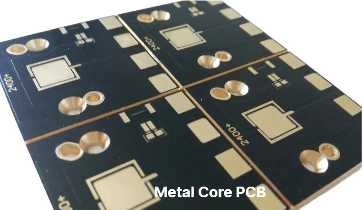
Metal Core PCB AssemblyMetal substrate PCBA utilizes aluminum or copper cores. Thermal conductive dielectric layers rapidly transfer component heat to the metal base layer for efficient thermal management. The thermal conductivity of the metal core (aluminum substrate > 2.0 W/mK) significantly exceeds that of FR-4. This enables direct contact with high-power AI chips (e.g., ASICs > 50W) and integration with external heat sinks via the metal layer, preventing performance degradation due to thermal throttling. These boards are commonly found in high-power AI acceleration modules, autonomous driving LiDAR systems, or edge computing devices, proving indispensable in scenarios requiring passive cooling within confined spaces.
Rigid-flex PCB assemblies integrate flexible PCBs (bendable, vibration-resistant) with rigid PCBs (supporting high-density components) into a single unit, achieving three-dimensional interconnections through chemical etching and lamination processes. The flexible section uses polyimide substrates capable of withstanding tens of thousands of dynamic bends without failure, replacing traditional connectors to reduce contact failures. In AI robot joints, drone vision systems, or wearable devices, rigid-flex boards connect sensors, processors, and power modules within limited space, enhancing system reliability and space utilization.
Core Technical Challenges in AI Hardware PCBA
Signal Integrity:At the core of AI hardware lies the parallel processing and exchange of massive data volumes. Its internal data buses, memory interfaces (such as GDDR6/HBM), and high-speed serial links (such as PCIe 5.0/6.0) all operate at frequencies in the GHz range. The first challenge facing signal integrity is attenuation. As high-frequency signals propagate through PCB transmission lines, they attenuate due to dielectric and conductor losses. Signal amplitude diminishes and edges become rounded—much like sound growing indistinct over long distances. To counter this, specialized low-loss-factor substrates like Panasonic's Megtron series or Rogers' Tachyon series must be employed. These materials maximize signal strength and integrity.
Another significant challenge is reflection and impedance mismatch. When signals encounter impedance discontinuities—such as vias, connectors, or corners—a portion of the energy reflects back toward the source, superimposing on subsequent signals and causing waveform distortion. This necessitates stringent impedance control during design. Every detail—from calculating trace width and dielectric thickness to selecting copper foil type—must be precise to ensure highly consistent impedance throughout the channel. Tolerances are typically controlled within ±5% or even tighter.
Furthermore, crosstalk acts like “whispering” between signal lines. When multiple high-speed lines are routed in parallel, energy from one line couples into adjacent lines via electric and magnetic fields, generating noise. To suppress crosstalk, the 3W rule (spacing between lines must be at least three times the line width) must be followed. Where necessary, protective ground planes should be added between critical networks, or a strip line stacking structure should be employed to leverage shielding effects. Ultimately, all these issues must be anticipated and resolved through precise simulation. Routing strategies, topology adjustments, and termination schemes should be optimized during the design phase to prevent irreversible errors on costly hardware.
Power Integrity:AI processors exhibit extreme power consumption dynamics, capable of switching from idle to full load states within milliseconds, generating transient current changes of tens to hundreds of amperes. These violent current fluctuations act like sudden “hurricanes,” posing extreme challenges to the power delivery network. The primary goal of power integrity is to maintain stable supply voltage. When massive transient currents flow through parasitic inductance present in the power network, they generate significant switching noise, causing instantaneous voltage dips or spikes. If these exceed the chip's tolerance, they can trigger logic errors or even system crashes.
Addressing this challenge requires constructing a low-impedance power delivery network. This relies on dedicated power and ground planes within multilayer PCBs, which form a distributed decoupling capacitance capable of rapidly responding to local current demands. Simultaneously, the layout and selection of decoupling capacitors are critical success factors. A combination of capacitors—ranging from low-frequency, high-capacitance types to high-frequency, low-capacitance variants—must be employed to form an efficient “capacitor bank.” Crucially, high-frequency decoupling capacitors must be placed as close as possible to the chip's power pins to minimize loop inductance. This ensures they can deliver power to the chip within nanoseconds, smoothing current fluctuations.
DC voltage drop is another critical issue. High currents flowing through copper traces in power delivery paths generate voltage drops due to trace resistance, potentially causing chips at distant locations to receive voltages below the required minimum. To address this, thicker copper traces (e.g., 2oz or 3oz) and wider traces are often employed for high-current paths. This reduces DC resistance, ensuring efficient, low-loss power delivery to every computational unit.
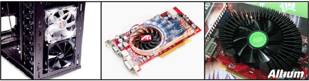
Thermal Management:Extremely high computing power density inevitably comes with extremely high power consumption, and nearly all of this power is ultimately converted into heat. AI chips exhibit astonishing thermal flux densities. If heat cannot be dissipated promptly, core temperatures will rapidly surge, leading to degraded transistor performance (reduced electron mobility), diminished reliability, and even triggering thermal protection that forces frequency throttling—directly limiting sustained computational output. Therefore, thermal management is not an afterthought but a core design element requiring comprehensive planning from the PCB layout stage.
The PCB itself serves as a critical thermal pathway. Beneath the chip, thousands of densely packed thermal vias—filled with thermal paste—function like miniature chimneys, efficiently conducting heat vertically to the PCB's reverse side. For extreme power scenarios, metal substrates (e.g., aluminum or copper boards) are the preferred choice. Their metallic core layers possess exceptional thermal conductivity, rapidly dispersing heat laterally before transferring it to external heat sinks or cold plates via thermal interface materials.
Ultimately, the PCB must serve as the cornerstone of the entire system-level thermal solution. Its design must seamlessly integrate with heat sinks, heat pipes, vapor chambers, and even complex water-cooling modules. The layout of high-power components (such as AI processors and memory) must thoroughly consider airflow paths and heat sink contact areas to prevent localized hotspots. Every minute design choice—from copper foil thickness to the number of heat dissipation holes—directly impacts whether the entire AI hardware can sustainably and stably deliver its peak performance.
High-speed digital circuits inherently generate significant electromagnetic interference. Rapidly changing currents and voltages produce broadband electromagnetic radiation, while the system itself remains highly susceptible to external interference or crosstalk between internal modules. EMC demands that AI hardware both limit its own electromagnetic emissions—preventing interference with other devices or exceeding regulatory thresholds—and withstand external electromagnetic disturbances to ensure stable operation in complex electromagnetic environments.
Achieving robust EMC fundamentally relies on establishing a clean, continuous reference ground plane. This ground plane provides the shortest, lowest-impedance path for return currents, minimizing antenna effects. For critical high-speed signal lines or noise sources, localized isolation via shielding enclosures is often necessary to confine electromagnetic energy within a confined space. Additionally, effective filtering circuits—such as π-type filters—must be implemented at power supply entry points and critical IC power pins to eliminate high-frequency noise on the power network. This prevents noise from radiating outward through power lines or interfering with other sensitive circuits. All these measures require meticulous design during the layout and routing phase, as many EMC issues become difficult to resolve once the board is manufactured.
How to Choose the Right PCBA
Selecting the right PCBA (Printed Circuit Board Assembly) supplier requires comprehensive consideration of multiple core dimensions, including technical capabilities, quality systems, delivery efficiency, service and cost structure, as well as industry suitability.
Technical capability forms the foundation. It is essential to ensure the supplier possesses the required process precision (e.g., high-density routing, microvia technology), supports the necessary PCB layer counts and materials (e.g., high-frequency boards, metal core boards), and can provide design support (e.g., DFM analysis).
Quality systems guarantee stability. Suppliers should hold international certifications (e.g., ISO9001, IATF16949), implement rigorous inspection processes (e.g., AOI, SPI, X-Ray), and maintain reliable quality data.
Delivery efficiency directly impacts project timelines. Focus on standard lead times, expedited service capabilities, and supply chain stability.
Service and cost requirements demand transparent quotations with no hidden fees, alongside effective engineering optimization and post-sales support.
Finally, industry alignment emphasizes that suppliers must possess proven success in relevant sectors (e.g., consumer electronics, automotive electronics).
It is recommended to conduct final evaluations through small-batch trial production and on-site inspections, selecting partners offering the optimal balance between performance, reliability, and cost.
Selecting the right high-speed PCBA is a critical step for the successful implementation of AI hardware. Whether it's server clusters pursuing extreme compute density or edge devices requiring a balance between performance and power consumption, circuit board solutions must be tailored to specific application scenarios. It is advisable to engage PCB suppliers with AI hardware expertise early in the project. Validate design feasibility through small-batch trial production and leverage simulation tools to optimize signal and power integrity. Only through rigorous design, appropriate material selection, and professional manufacturing processes can a stable, reliable, high-performance AI hardware platform be built—providing a solid computational foundation for artificial intelligence applications.
One-Stop HDI PCB Manufacturer and Its PCB Via Filing Capabilities
If you're looking for turnkey HDI electronics manufacturing services (EMS) from hardware development to PCBA fabrication and box-build assembly, you can work with the one-stop HDI PCBA manufacturer PCBONLINE.
Founded in 1999, PCBONLINE has R&D capabilities for HDI projects and EMS manufacturing capabilities, including via filling for stacked vias. It provides 4-to-64-layer HDI PCB fabrication, assembly, and PCBA box-build assembly. You can order various HDI PCBs from PCBONLINE, such as FR4, polyimide (flexible PCB), polyimide + FR4 (rigid-flex PCB), and PTFE/Rogers (high-frequency PCB).

3000m² of production capacity per day for HDI PCBs with builds of 1+N+1, 2+N+2, 3+N+3,4+N+4, and arbitrary interconnection in any layers.
PCBONLINE has hardware and software R&D capabilities for IoT applications requiring HDI design, including PCBA and enclosures.
We can manufacture complex PCBs with stacker vias, via-in-pad, microvias, inlay boards, heavy copper designs, and hybrid and fine structure lay-ups.
Besides HDI PCB fabrication, we have powerful capabilities in fine-pitch assembly for HDI PCB assembly.
We have rich R&D and manufacturing experience for HDI applications such as FPGA boards.
High-quality HDI PCB and PCBA manufacturing certified with ISO 9001:2015, IATF 16949, RoHS, REACH, UL, and IPC-A-610 Class 2/3.
Here'e the PCB via filing capabilities at PCBONLINEL:
- Micriavia filling with copper: laser via size 0.1-0.125mm, priority 0.1mm
- Finished hole size for via-in-pad filling with resin: 0.1-0.9mm (drill size 0.15-1.0mm), 0.3-0.55mm normal (drill size 0.4-0.65mm)
- Max aspect ratio for via-in-pad filling with resin PCB - 12: 1
- Min resin plugged PCB thickness: 0.2mm
- Max via-filling ith resin PCB thickness: 3.2mm
- Making different hole sizes with via filling in one board: Yes
- Via filling with copper/silver: Yes
If you need HDI PCBAs or any other PCBAs requiring via filling, please send your email to PCBONLINE at info@pcbonline.com. We will provide one-on-one engineering support to you.
Conclusion
Via filling is used for creating stacked vias in HDI PCB fabrication, BGA/CSP/QFN IC packaging, and filling PCB via-in-pad with resin during multilayer PCB fabrication. If you need one-stop electronics manufacturing for your HDI PCBA project, contact the one-stop advanced PCB manufacturer PCBONLINE for high-quality PCBA and box-build solutions tailored to your project's needs.
PCB fabrication at PCBONLINE.pdf


