
Printed circuit boards (PCBs) are the core backbone of electronic products, and every step in their manufacturing process is crucial. Despite continuous technological advancements, various process issues can arise at every step, from inner layer fabrication and drilling and plating to final surface treatment and molding. This section aims to systematically identify these common manufacturing challenges and provide practical solutions. We will explore in detail how to overcome these challenges through precise parameter control, optimized equipment and material selection, and rigorous process flow, thereby ensuring the production of high-quality and reliable PCB products.
In this article:
Part 1. PCB Fabrication Process Part 2. Common Process Problems Part 3. Corresponding SolutionsPCB Fabrication Process
Printed Circuit Board (PCB) fabrication is a complex process that transforms design files into physical circuit boards. This process can generally be summarized into the following key stages.First, internal layer fabrication and lamination. After the design files are reviewed, the factory applies the circuit pattern to the internal layers of the copper-clad laminate using chemical processes such as photolithography, development, and etching. For multilayer boards, these fabricated internal layers are precisely aligned and laminated together with prepreg and copper foil under high temperature and high pressure to form a solid, integrated structure.
Next, drilling and plating are crucial steps for achieving electrical connections between different layers. High-speed drills or laser drills are used to create various holes, including through-holes connecting different layers, in the laminated board. Subsequently, a layer of copper is deposited on the inner walls of these holes and on the outer copper layers through electroless copper deposition and electroplating processes, ensuring conductivity and continuity of all traces.
Finally, surface treatment and molding are performed. After plating, the PCB is coated with solder mask to protect the traces and printed with silkscreen information such as component identification. To ensure good solderability and prevent copper oxidation, surface treatments such as tin spraying or gold deposition are performed. Finally, after electrical testing and strict quality inspection, qualified boards are cut into the required size and finally packaged.
Common Process Problems
1. Internal Layer Fabrication and LaminationUneven Line Width/Space: During the image transfer or etching process, improper control of exposure time, developer concentration, or etching solution temperature can cause copper line width or line spacing to deviate from the designed values. Severe deviations can result in open circuits (lines too thin) or short circuits (lines too thick, spacing too small).
Copper slag residue: Incomplete etching can leave copper slag on the board surface, which can cause short circuits during subsequent lamination or electrical testing.
Interlayer misalignment: Before lamination of a multilayer board, if the layers (including internal layers and prepreg) are not accurately aligned, the through-holes in the final board may not accurately connect to the internal layer pads, resulting in open circuits.
2. Drilling and PlatingDrilling misalignment: If the drill rig is misaligned or the drill bit itself deviates, the drilled holes may deviate from the designed position. This can prevent the subsequent plated holes from accurately connecting to the internal pads, resulting in open circuits.
Rough hole walls: Improper drilling parameters (such as rotation speed and feed rate) or drill bit wear can result in rough hole walls. Rough hole walls can affect the quality of subsequent copper deposition, potentially leading to uneven or discontinuous electroplating.
Copper skipping: During the electroless copper deposition process, if the hole walls are not adequately cleaned or the copper plating solution is insufficiently active, the hole walls may lack a complete copper layer, making subsequent electroplating impossible and causing open circuits within the hole.
Uneven electroplating or cracking within the hole: Uneven current distribution or unstable plating solution composition during electroplating can result in uneven copper layer thickness within the hole. Under stress (such as thermal shock), thinner copper layers may crack, causing open circuits within the hole.
3. Surface Treatment and FormingPoor solder mask adhesion or bubbles: Uneven solder mask ink application, insufficient exposure, or incomplete curing can result in poor solder mask adhesion and easy peeling. Air bubbles mixed into the ink can also affect the integrity of the solder mask, reducing its protective effect on the circuit.
Blurred or flaked silkscreen: Improper silkscreen ink viscosity or poorly controlled printing processes can cause blurred characters and logos. Incomplete curing results in poor adhesion of the silkscreen layer, making it prone to peeling during use.
Uneven or oxidized surface finish: During the hot air leveling (HASL) process, uneven hot air pressure can lead to inconsistent tin layer thickness. In the electroless nickel (ENIG) process, improper chemical composition can result in an excessively thin gold layer or a black disk effect, impacting solderability.
Molding burrs: During CNC milling or stamping, if the tool or die is not sharp or the parameters are incorrectly set, uneven burrs can be left on the board edge. These burrs not only affect the appearance but can also cause short circuits or operator injuries during assembly.
Warping or distortion of the board: Improper temperature and pressure control during lamination, or uneven stress on the board during subsequent heating, can cause warping or distortion of the PCB. This can seriously affect the quality of subsequent component placement and soldering.
Corresponding Solutions
1. Solutions for Internal Layer Fabrication and Lamination· Uneven Line Width/Space: Solving this problem requires strict control of process parameters for photolithography, development, and etching. Using high-precision exposure equipment, regularly changing and testing chemical solutions (such as developer and etchant), and maintaining constant temperature and speed ensures accurate circuit pattern formation.
· Copper slag residue: This problem is typically addressed by optimizing the etching process. Increasing etching solution circulation and spray pressure to ensure effective rinsing of the board surface, and thoroughly cleaning the board, can effectively remove copper slag.
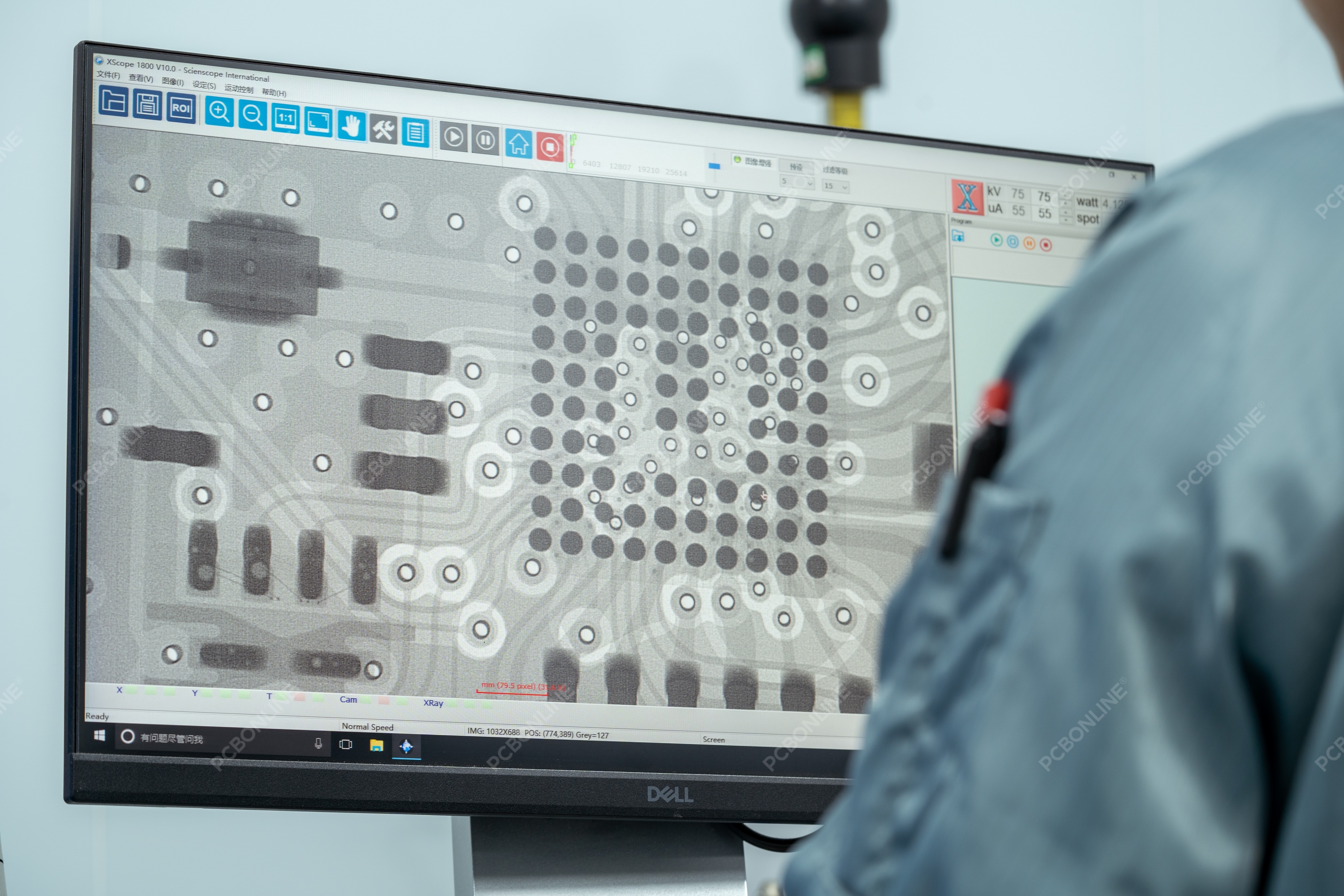
· Layer misalignment: The key to resolving layer misalignment lies in high-precision alignment. Before lamination, an X-ray automated alignment system precisely aligns the inner layer panels and drilled holes, ensuring accurate placement of each layer.
· Drilling deviation: Use a high-precision CNC drill and regularly calibrate the drill and drill bit. For high-density interconnect (HDI) boards, laser drilling technology can be used, which offers higher precision and effectively avoids the deviations associated with mechanical drilling.
· Hole wall roughness: Select a high-quality drill bit and set optimal drilling parameters (such as rotation speed and feed rate) for different materials. Effective post-drilling desmear treatment, such as plasma or chemical desmear treatment, ensures clean and smooth hole walls, facilitating subsequent electroplating.
· Copper skipping: Before copper deposition, the hole walls must be thoroughly cleaned and activated. Using ultrasonic cleaning and a high-quality activation solution ensures a uniform and continuous catalyst layer on the hole walls, thus ensuring optimal copper deposition results.
· Uneven electroplating or cracks within the hole: By optimizing the plating tank design, adjusting the plating solution composition and additives, and controlling the current density, you can ensure uniform thickness of the electroplated layer within the hole and on the board surface. At the same time, the use of advanced technologies such as pulse plating can also effectively improve the density and toughness of the electroplating layer and prevent breakage.
3. Solutions for Surface Treatment and Forming· Poor solder mask adhesion or bubbles: Before applying solder mask ink, thoroughly clean the board surface and ensure that no bubbles are introduced during the application, exposure, and curing processes. Precisely controlling the UV exposure dose and curing temperature ensures a secure bond between the solder mask and the board.
· Blurred or peeling silk screen printing: Use high-quality silk screen ink and adjust its viscosity to suit printing conditions. Ensuring that the curing temperature and time after silk screen printing meet the required standards can enhance the wear resistance and adhesion of the silk screen layer.
· Uneven or oxidized surface finish: Different surface treatment processes require strict monitoring of the chemical composition and temperature. For example, in the gold deposition process, the gold salt needs to be regularly tested and replenished to maintain a stable gold layer thickness. For HASL, controlling the hot air pressure ensures the smoothness of the tin layer.
· Forming burrs: Regularly replace worn milling cutters or dies. Selecting appropriate milling paths and parameters, or using non-contact technologies such as laser cutting, can effectively reduce board edge burrs.
Board warping or distortion: This problem is primarily addressed by controlling the lamination process and material stress. Ensuring symmetrical arrangement of the layers during lamination and performing multiple stress relief treatments during board production, such as baking at different stages, can effectively reduce board warping.
From initial uneven line width and spacing, to complex inter-layer misalignment and in-hole plating defects, to final board warpage and burr problems, each challenge reflects the complexity of process control. However, as detailed in this article, these problems can be effectively addressed through the use of high-precision equipment, optimized chemical formulations, strict quality management, and the introduction of advanced automation technology.
One-Stop HDI PCB Manufacturer and Its PCB Via Filing Capabilities
If you're looking for turnkey HDI electronics manufacturing services (EMS) from hardware development to PCBA fabrication and box-build assembly, you can work with the one-stop HDI PCBA manufacturer PCBONLINE.
Founded in 1999, PCBONLINE has R&D capabilities for HDI projects and EMS manufacturing capabilities, including via filling for stacked vias. It provides 4-to-64-layer HDI PCB fabrication, assembly, and PCBA box-build assembly. You can order various HDI PCBs from PCBONLINE, such as FR4, polyimide (flexible PCB), polyimide + FR4 (rigid-flex PCB), and PTFE/Rogers (high-frequency PCB).

3000m² of production capacity per day for HDI PCBs with builds of 1+N+1, 2+N+2, 3+N+3,4+N+4, and arbitrary interconnection in any layers.
PCBONLINE has hardware and software R&D capabilities for IoT applications requiring HDI design, including PCBA and enclosures.
We can manufacture complex PCBs with stacker vias, via-in-pad, microvias, inlay boards, heavy copper designs, and hybrid and fine structure lay-ups.
Besides HDI PCB fabrication, we have powerful capabilities in fine-pitch assembly for HDI PCB assembly.
We have rich R&D and manufacturing experience for HDI applications such as FPGA boards.
High-quality HDI PCB and PCBA manufacturing certified with ISO 9001:2015, IATF 16949, RoHS, REACH, UL, and IPC-A-610 Class 2/3.
Here'e the PCB via filing capabilities at PCBONLINEL:
- Micriavia filling with copper: laser via size 0.1-0.125mm, priority 0.1mm
- Finished hole size for via-in-pad filling with resin: 0.1-0.9mm (drill size 0.15-1.0mm), 0.3-0.55mm normal (drill size 0.4-0.65mm)
- Max aspect ratio for via-in-pad filling with resin PCB - 12: 1
- Min resin plugged PCB thickness: 0.2mm
- Max via-filling ith resin PCB thickness: 3.2mm
- Making different hole sizes with via filling in one board: Yes
- Via filling with copper/silver: Yes
If you need HDI PCBAs or any other PCBAs requiring via filling, please send your email to PCBONLINE at info@pcbonline.com. We will provide one-on-one engineering support to you.
Conclusion
Via filling is used for creating stacked vias in HDI PCB fabrication, BGA/CSP/QFN IC packaging, and filling PCB via-in-pad with resin during multilayer PCB fabrication. If you need one-stop electronics manufacturing for your HDI PCBA project, contact the one-stop advanced PCB manufacturer PCBONLINE for high-quality PCBA and box-build solutions tailored to your project's needs.
PCB fabrication at PCBONLINE.pdf


