
In the intelligent era, data is being generated around us at an unprecedented rate. From sensors in smart factories to cameras in unmanned supermarkets, these scenarios demand faster and more reliable computing. This is the root of the rise of "edge computing," and the physical entities that carry this computing power are "edge devices." This article will delve into the crucial manufacturing partners behind a successful edge device: PCB OEMs. How do they start from a blueprint, through precision manufacturing and rigorous testing, ultimately reliably deploying these intelligent "brains" into every corner of our lives?
In this article:
Part 1. What is Edge Device Part 2. What is PCB OEM? Part 3. How do PCB OEMs Produce Edge Devices? Part 4. OEMs' Production CapabilitiesWhat is Edge Device
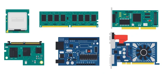
Edge devices are intelligent devices that perform data computing and processing at the "edge" of the physical world (close to where the data is generated or where it's used), rather than transmitting all data to a distant cloud.
You can think of them as "localized, small intelligent brains."
To better understand this, let's compare traditional (cloud computing) and modern (edge computing) approaches:
Traditional Cloud Computing (uploading everything):
Imagine an old-fashioned supermarket. Each customer couldn't calculate their own payment for each item they took. Instead, they had to go to the main service counter (in the cloud) in the center of the supermarket to queue, scan a QR code, and pay. If there were many customers, the service counter would be extremely congested (network latency), resulting in long queues (slow response). Furthermore, if the service counter were to fail (network outage), the entire supermarket would cease operations.
Edge Computing (local processing):
This is the modern supermarket we're familiar with. Each shelf area has multiple checkout counters (edge devices). Customers pay locally, which is very fast (low latency). Even if one checkout counter fails, it doesn't affect other areas (high reliability). The main service counter (in the cloud) is only contacted for complex tasks like membership points and bulk purchases.
In this metaphor, each local checkout counter is an “edge device.”
What is PCB OEM?
PCB OEM stands for "original equipment manufacturing of printed circuit boards." This refers to a partnership model in which a brand provides design drawings, and a specialized factory strictly follows the drawings to procure materials, manufacture the boards, assemble components, and finally deliver the finished boards to the brand.
Developing edge devices requires extending the value chain upstream and downstream, transforming from a simple "manufacturing service provider" to an "edge computing solution provider."
How do PCB OEMs Produce Edge Devices?
Blueprint Optimization
This is far more than just drawing a circuit diagram. Because edge devices inherently require local intelligent processing in harsh environments, OEM partners need to be involved from the outset and work with the brand to review requirements: What temperature, humidity, and vibration will the device face? How much AI computing power is required? What is the power consumption budget? During this stage, both parties work together to refine not only the logical connections of the circuit but also the physical structure of the product (PCB layout) and the bill of materials (BOM). This is an iterative process, using simulation to predict signal integrity, power integrity, and thermal performance to ensure the design is theoretically rock-solid.

Manufacturing and Verification Phase
OEMs convert design files into actual circuit boards, procure the specified components, and use high-precision placement machines to solder thousands of these components onto the boards, creating a PCBA. But this is more than just "production." For edge devices, a simple power-on check is not enough. A rigorous "simulated test" is required: testing stability under stressful conditions such as high and low temperatures and continuous operation; verifying that computing power meets requirements; and checking that all interfaces can transmit data accurately.
Mass Production
OEMs start production lines and scale manufacturing, but their work doesn't end there. They continuously monitor production yields and manage the complex component supply chain to prevent production halts due to chip shortages. They also provide long-term lifecycle management. Even if certain components are discontinued in the future, they will help identify and verify alternatives, ensuring the stable supply of this edge device in the market for years to come.
OEMs' Production Capabilities
Complex Design and Supply Capabilities
- Experience in manufacturing complex PCBs: You need to examine the manufacturer's ability to mass-produce high-density interconnect (HDI) boards, expertise in high-speed signal processing (e.g., differential pairs, impedance control), and experience with high-frequency/high-speed boards (e.g., Rogers and Tyconic). These are the physical foundations for ensuring AI computing power and signal integrity.
- Strong design engineering (DFM/DFA) capabilities: A good OEM manufacturer won't passively wait for drawings. They should proactively provide design for manufacturability (DFM) and design for assembly (DFA) feedback, identifying potential design issues that could lead to low yield, high cost, or reliability issues early on. For example, they might recommend optimizing component layout for improved heat dissipation or adjusting routing to avoid signal interference.
- Advanced supply chain and material management: Edge devices often utilize specialized control chips. Manufacturers must have stable, authorized component procurement channels and the ability to adapt to supply chain fluctuations to ensure production isn't stalled due to a single missing chip.
Quality and Reliability Assurance
- Testing System: Don't be content with just basic electrical testing. Ask the manufacturer whether they offer flying probe testing/bed-of-nails testing, in-circuit testing (ICT), functional testing (FCT), and the more critical environmental stress screening (ESS)—which uses high-temperature cycling and vibration testing to screen out premature failures and simulate years of wear and tear on the equipment.
- Comprehensive Quality Certifications: International standard certifications are a testament to their capabilities. ISO 9001 (Quality Management System) is the foundation, while IATF 16949 (Automotive) or ISO 13485 (Medical) demonstrate that their quality system meets higher standards. This is especially important if your product has specific industry standards.
- Traceability: Traceability should be maintained at every stage, from raw materials to finished product. When quality issues arise, the problem batch can be quickly identified, the root cause analyzed, and effective recalls or corrective measures implemented.
Communication Efficiency
- Communication Efficiency and Transparency: Evaluate their project management system. Does they have a dedicated project manager? Is communication smooth and timely (language proficiency is also crucial)? Can they provide transparent production progress reports and yield data?
- Smooth Transition from Prototype to Mass Production: The manufacturer should be able to efficiently support small-batch prototyping and, once the design is finalized, seamlessly transition to large-scale production. The accumulated experience and data transfer during this process are crucial.
- Flexibility: Can they adapt to your engineering changes? Can they handle urgent order adjustments? A flexible manufacturer can help you seize opportunities in a rapidly changing market.
Total Cost of Ownership
- Cost Transparency: Excellent manufacturers will help you analyze your costs and propose reasonable cost reduction solutions (such as through component substitution or design optimization), rather than blindly cutting prices and risking quality.
- Geography and Logistics: While location is no longer as crucial as it once was, manufacturers located near each other often have advantages in communication, logistics speed, and control of supply chain risks. A trade-off between cost and efficiency/risk is crucial.
- Long-Term Lifecycle Management: Electronic components have end-of-life cycles. Reliable OEMs will proactively notify you of component lifecycle status and assist with last-time-buy or replacement component verification, ensuring your product's continued market availability for many years.
In short, edge devices represent the transfer of computing power from the cloud to every corner of the real world, and are a key component in realizing the intelligent future of everything. Choosing the right PCB OEM partner means finding a strategic ally capable of transforming innovative designs into robust products. This journey from concept to reality goes far beyond simple PCB production; it's a comprehensive test of technical depth, quality assurance, and collaborative trust.
One-Stop HDI PCB Manufacturer and Its PCB Via Filing Capabilities
If you're looking for turnkey HDI electronics manufacturing services (EMS) from hardware development to PCBA fabrication and box-build assembly, you can work with the one-stop HDI PCBA manufacturer PCBONLINE.
Founded in 1999, PCBONLINE has R&D capabilities for HDI projects and EMS manufacturing capabilities, including via filling for stacked vias. It provides 4-to-64-layer HDI PCB fabrication, assembly, and PCBA box-build assembly. You can order various HDI PCBs from PCBONLINE, such as FR4, polyimide (flexible PCB), polyimide + FR4 (rigid-flex PCB), and PTFE/Rogers (high-frequency PCB).

3000m² of production capacity per day for HDI PCBs with builds of 1+N+1, 2+N+2, 3+N+3,4+N+4, and arbitrary interconnection in any layers.
PCBONLINE has hardware and software R&D capabilities for IoT applications requiring HDI design, including PCBA and enclosures.
We can manufacture complex PCBs with stacker vias, via-in-pad, microvias, inlay boards, heavy copper designs, and hybrid and fine structure lay-ups.
Besides HDI PCB fabrication, we have powerful capabilities in fine-pitch assembly for HDI PCB assembly.
We have rich R&D and manufacturing experience for HDI applications such as FPGA boards.
High-quality HDI PCB and PCBA manufacturing certified with ISO 9001:2015, IATF 16949, RoHS, REACH, UL, and IPC-A-610 Class 2/3.
Here'e the PCB via filing capabilities at PCBONLINEL:
- Micriavia filling with copper: laser via size 0.1-0.125mm, priority 0.1mm
- Finished hole size for via-in-pad filling with resin: 0.1-0.9mm (drill size 0.15-1.0mm), 0.3-0.55mm normal (drill size 0.4-0.65mm)
- Max aspect ratio for via-in-pad filling with resin PCB - 12: 1
- Min resin plugged PCB thickness: 0.2mm
- Max via-filling ith resin PCB thickness: 3.2mm
- Making different hole sizes with via filling in one board: Yes
- Via filling with copper/silver: Yes
If you need HDI PCBAs or any other PCBAs requiring via filling, please send your email to PCBONLINE at info@pcbonline.com. We will provide one-on-one engineering support to you.
Conclusion
Via filling is used for creating stacked vias in HDI PCB fabrication, BGA/CSP/QFN IC packaging, and filling PCB via-in-pad with resin during multilayer PCB fabrication. If you need one-stop electronics manufacturing for your HDI PCBA project, contact the one-stop advanced PCB manufacturer PCBONLINE for high-quality PCBA and box-build solutions tailored to your project's needs.
PCB fabrication at PCBONLINE.pdf


