
In printed circuit board design, a robust and reliable grounding system is fundamental to ensuring stable, noise-free operation of electronic devices. The ground bus serves as the backbone of this system. Whether implemented as a wide copper trace or an entire ground plane layer, understanding its principles, common configurations, and potential design pitfalls is crucial for every engineer and enthusiast. This article will delve into the core role of PCB ground buses and reveal common mistakes that can lead to degraded circuit performance or even failure.
In this article:
Part 1. What is Ground Bus in PCB? Part 2. Purpose and Function of the PCB Ground Bus Part 3. Common Forms Part 4. Four Common MistakesWhat is Ground Bus in PCB?
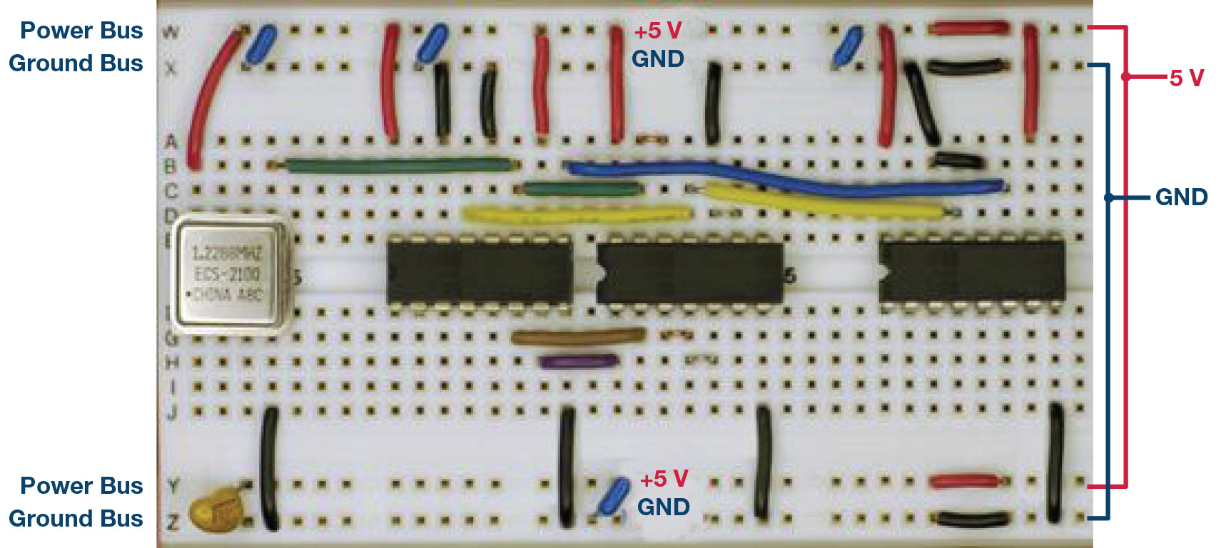
A PCB ground bus refers to a relatively wide and thick copper trace on a PCB. Its primary function is to serve as a common low-impedance return path for all component pins or signals requiring ground (GND).
If this seems abstract, imagine it as an “electrical highway” where all vehicles ultimately terminate at “ground.” The wider and smoother this highway (i.e., the lower its impedance), the less prone traffic becomes to congestion (i.e., the smaller the voltage fluctuations), resulting in a more stable overall system.
Purpose and Function of the PCB Ground Bus
The primary purpose and function of the PCB ground bus is to provide the entire circuit system with a low-impedance, stable, and clean common reference potential and current return path. It collects all ground currents flowing back to the power supply via wide copper traces or a continuous ground plane. Its low-impedance characteristics effectively suppress voltage fluctuations (ground bounce noise) caused by transient high currents, thereby ensuring signal integrity and providing a reliable reference for all voltage measurements. Simultaneously, by controlling the return current path and minimizing loop area, it suppresses electromagnetic interference (EMI) and enhances the system's immunity to interference. Ultimately, this ensures stable and reliable circuit operation.
Common Forms
PCB ground buses primarily take two common forms:Explicit wide traces were a common grounding method in early single-sided and simple double-sided PCBs. Due to limited layer resources preventing a full ground plane layer, designers would manually draw an exceptionally wide copper trace along the PCB edge or in specific areas to serve as the main trunk line for all ground connections. This approach offers low cost and simple implementation. However, it remains fundamentally a “line” with relatively high impedance and limited current return paths, resulting in weaker noise immunity. It is typically reserved for low-frequency or simple circuits with minimal signal integrity requirements.
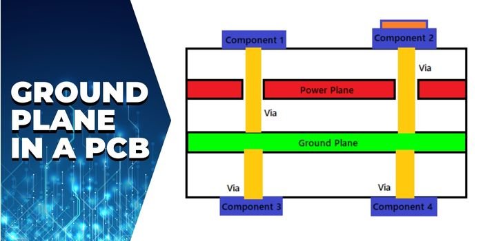
The ground plane represents the standard practice in modern multilayer board design, embodying the more advanced “surface” grounding concept. It involves completely covering an entire layer (or a significant portion of a layer) of the PCB with copper foil and defining it as a ground network, thereby forming a large, continuous low-impedance reference plane. All component ground pins connect directly to this plane via vias, providing an infinite number of parallel return paths for current. This configuration offers significant advantages: it delivers the lowest possible impedance and optimal signal integrity while providing excellent electromagnetic shielding and thermal dissipation. It is an indispensable design foundation for handling high-speed, high-density, and mixed-signal circuits.
Four Common Mistakes
1. Consult the Datasheet: This is the most critical step. Different models and brands of regulators may have specific requirements. The “Typical Application Circuit” section in the datasheet provides the official blueprint for polarity.
2. Verify Polarized Component Orientation: The direction of electrolytic capacitors, tantalum capacitors, and diodes is paramount in polarity operations. Double-check these components repeatedly. Before powering on, use the continuity setting on a multimeter to double-check for direct shorts.
3. Provide Correct Bias: Whether through a resistor network (e.g., LM317) or a feedback loop (e.g., switching regulator), supplying the chip with the bias conditions necessary for proper operation constitutes “polarization.”
4. Perform gradual power-up testing: For initial power-on, employ a “smoke test” (a humorous reference to preventing smoke) method: Use an adjustable current-limited power supply, initially set voltage and current limits low to observe if operating current is normal, then gradually increase to design values.
In summary, the PCB ground bus is far more than a simple connecting line; it serves as the cornerstone of the entire circuit design, responsible for maintaining signal purity and system stability. From explicit thick traces to complete ground planes, its evolution reflects an unrelenting pursuit of lower impedance and higher performance. Successful design hinges on strict adherence to core principles: low-impedance paths, star-shaped grounding, decoupling capacitor placement, and mixed-signal partitioning. By avoiding common design pitfalls, you can significantly enhance circuit immunity to interference, reduce electromagnetic radiation, and ensure the reliability of the final product.
One-Stop HDI PCB Manufacturer and Its PCB Via Filing Capabilities
If you're looking for turnkey HDI electronics manufacturing services (EMS) from hardware development to PCBA fabrication and box-build assembly, you can work with the one-stop HDI PCBA manufacturer PCBONLINE.
Founded in 1999, PCBONLINE has R&D capabilities for HDI projects and EMS manufacturing capabilities, including via filling for stacked vias. It provides 4-to-64-layer HDI PCB fabrication, assembly, and PCBA box-build assembly. You can order various HDI PCBs from PCBONLINE, such as FR4, polyimide (flexible PCB), polyimide + FR4 (rigid-flex PCB), and PTFE/Rogers (high-frequency PCB).

3000m² of production capacity per day for HDI PCBs with builds of 1+N+1, 2+N+2, 3+N+3,4+N+4, and arbitrary interconnection in any layers.
PCBONLINE has hardware and software R&D capabilities for IoT applications requiring HDI design, including PCBA and enclosures.
We can manufacture complex PCBs with stacker vias, via-in-pad, microvias, inlay boards, heavy copper designs, and hybrid and fine structure lay-ups.
Besides HDI PCB fabrication, we have powerful capabilities in fine-pitch assembly for HDI PCB assembly.
We have rich R&D and manufacturing experience for HDI applications such as FPGA boards.
High-quality HDI PCB and PCBA manufacturing certified with ISO 9001:2015, IATF 16949, RoHS, REACH, UL, and IPC-A-610 Class 2/3.
Here'e the PCB via filing capabilities at PCBONLINEL:
- Micriavia filling with copper: laser via size 0.1-0.125mm, priority 0.1mm
- Finished hole size for via-in-pad filling with resin: 0.1-0.9mm (drill size 0.15-1.0mm), 0.3-0.55mm normal (drill size 0.4-0.65mm)
- Max aspect ratio for via-in-pad filling with resin PCB - 12: 1
- Min resin plugged PCB thickness: 0.2mm
- Max via-filling ith resin PCB thickness: 3.2mm
- Making different hole sizes with via filling in one board: Yes
- Via filling with copper/silver: Yes
If you need HDI PCBAs or any other PCBAs requiring via filling, please send your email to PCBONLINE at info@pcbonline.com. We will provide one-on-one engineering support to you.
Conclusion
Via filling is used for creating stacked vias in HDI PCB fabrication, BGA/CSP/QFN IC packaging, and filling PCB via-in-pad with resin during multilayer PCB fabrication. If you need one-stop electronics manufacturing for your HDI PCBA project, contact the one-stop advanced PCB manufacturer PCBONLINE for high-quality PCBA and box-build solutions tailored to your project's needs.
PCB fabrication at PCBONLINE.pdf


