
In the fast-paced world of electronics development, where every hour counts, the ability to swiftly transform a design concept into a functional prototype is a critical competitive advantage. Quickturn PCB Assembly has emerged as the cornerstone of this accelerated innovation cycle. This service is far more than just speedy manufacturing; it represents a sophisticated, integrated ecosystem designed to compress the entire journey from digital files to tested assemblies into a matter of days. By seamlessly combining rapid fabrication, agile supply chain management, and flexible, high-mix production lines, Quickturn PCB Assembly empowers engineers and companies to validate, iterate, and launch with unprecedented speed. The following exploration details how this vital service works, from the essential files that set it in motion to the advanced welding processes that ensure reliability, ultimately enabling the rapid realization of tomorrow's technology today.
In this article:
Part 1. What is Quickturn PCB Assembly Part 2. Supported Welding Processes Part 3. What Documents are RequiredWhat is Quickturn PCB Assembly
Quickturn PCB Assembly is a critical component in modern electronic hardware development workflows. It is not merely a single-step acceleration but an end-to-end solution integrating ultra-fast board manufacturing, agile material sourcing, flexible production lines, and efficient engineering management. Its fundamental purpose is to convert customer design files (such as Gerber, BOM, and coordinate files) into fully assembled printed circuit board assemblies (PCBA) ready for functional testing within days or even hours (typical lead times range from 24 hours to 5 business days), thereby meeting specific urgent demands throughout the product lifecycle. This service model is driven by the intensifying competitive landscape in the electronics industry, where product iteration cycles are drastically compressed. Companies must adopt a “rapid trial-and-error, rapid validation” approach to seize market opportunities. Thus, the success of Quickturn PCB Assembly hinges on service providers establishing a highly collaborative and digital ecosystem: Upon receiving design files, automated engineering analysis software simultaneously initiates design for manufacturability reviews and component sourcing feasibility assessments to identify potential bottlenecks. Concurrently, leveraging extensive supply chain networks and strategic inventory, providers activate emergency material procurement—even utilizing reserve stocks for common components—to mitigate risks associated with long-lead-time parts. During production, flexible manufacturing cells and highly automated SMT lines enable rapid switching between different products. Technologies like no-clean processes, laser stenciling, and inline SPI/AOI inspection are widely adopted, significantly reducing process setup and quality inspection times while maintaining quality standards. At its core, this service transcends mere “contract manufacturing.” It empowers innovation teams by leveraging the provider's robust supply chain resilience, advanced manufacturing capabilities, and project management expertise. This enables startups, R&D departments, or academic institutions to validate design feasibility with minimal initial costs and risks, rapidly obtaining physical prototypes for demonstrations, testing, or even small-batch crowdfunding campaigns. However, achieving true “Quickturn” poses significant challenges: it relies heavily on the accuracy and standardization of customer design files, where any oversight or material information error can cause the entire rapid process to fail and incur cost overruns. Simultaneously, it tests the service provider's comprehensive capabilities in handling unexpected supply chain disruptions, managing highly complex designs (such as HDI and dense BGAs), and balancing the speed, cost, and quality triangle. Therefore, Quickturn PCB Assembly represents a highly specialized, time-value-centric advanced service model within modern electronics manufacturing.

Supported Welding Processes
1. Surface Mount Technology (SMT)This is the dominant process in rapid assembly, suitable for the vast majority of modern electronic components.
Principle and Process: Using high-precision placement machines, minute surface-mount components (such as resistors, capacitors, ICs, etc.) are precisely positioned onto solder paste-printed pads on PCBs. These are then passed through a reflow oven, where the solder paste melts, cools, and forms reliable electrical and mechanical connections.
Advantages at Quickturn:
High-Speed Automation: Ideal for rapid batch assembly, forming the core of “quick” delivery.
- High-Density Integration: Capable of handling ultra-small or bottom-lead packages like 01005, BGA, QFN, and CSP to meet compact design requirements.
- Consistent Quality: Controllable reflow soldering parameters, combined with SPI (Solder Paste Inspection) and AOI (Automated Optical Inspection), effectively ensure soldering quality and reduce rework time.

Complementing SMT, this method handles components requiring high mechanical strength or high power.
Principle and Process: Components with leads are inserted into drilled holes in the PCB, then soldered via wave soldering (for entire board bottom surfaces) or selective wave soldering (for specific locations). Manual soldering is also common for extremely small-batch prototyping.
Challenges and Solutions in Quickturn:
- Automation vs. Flexibility: Wave soldering suits volume production but requires fixture setup time. Thus, Quickturn providers typically maintain selective wave soldering equipment or skilled hand-soldering teams to flexibly handle small-batch, high-variety THT components, avoiding lead time delays caused by fixtures.
- Hybrid Processes: Most boards incorporate both SMT and THT components. The standard workflow is “SMT reflow first, followed by THT soldering.” Optimizing this sequence is critical for ensuring efficiency and quality.

This is an indispensable flexible and remedial process in rapid prototyping.
- Application Scenarios:
Ultra-low volume or single boards: When automated setup time is uneconomical, the entire process is performed manually by experienced technicians.
Post-Assembly: Components intolerant to high temperatures, such as connectors and interfaces, are manually soldered after the main reflow process.
Engineering Changes & Debugging: During prototype validation, temporary component replacements, flying leads, or test point additions.
Repair & Board Salvage: Precise remediation of individual soldering defects (e.g., cold solder joints, bridging) detected by AOI or testing to salvage entire boards—critical for high-value prototypes.
4. Specialized Soldering and Auxiliary ProcessesTo address complex, high-reliability design requirements, advanced Quickturn service providers also employ the following techniques:
Principles and Special Applications:
- Crimp Technology: Used for high-speed backplane connectors, achieving hermetic connections through precision mechanical pressure without heating, ensuring signal integrity.
- Underfill: Special adhesive injected beneath chips (especially large BGAs). Upon curing, it uniformly distributes thermal expansion stresses between the chip and PCB, significantly enhancing reliability and drop resistance in harsh environments. Commonly used in mobile devices and automotive electronics prototypes.
- Triple-Proof Coating: After assembly, a protective coating is sprayed onto the board surface to provide moisture resistance, corrosion resistance, and mold resistance. Suitable for prototype validation in outdoor, industrial, or high-humidity environments.
What Documents are Required
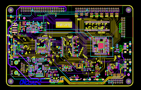
When initiating a Quickturn PCB Assembly project, the files provided by the customer form the foundation for ensuring the entire process is executed accurately and efficiently. Together, these files constitute a complete set of production instructions, and any missing or erroneous data may lead to delivery delays or increased costs. First, the customer must supply comprehensive PCB production files, typically centered around Gerber files. These serve as the standard language for describing circuit graphics across layers, including the trace layer, solder mask layer, silkscreen layer, and drill patterns. The accuracy of Gerber files directly determines the manufacturing quality of the PCB itself; even minor deviations can cause critical issues like open circuits or short circuits. The accompanying drill files precisely specify the location and dimensions of through-holes and vias, which are particularly crucial for high-density interconnect designs. Together, these files form the physical framework of the circuit board.
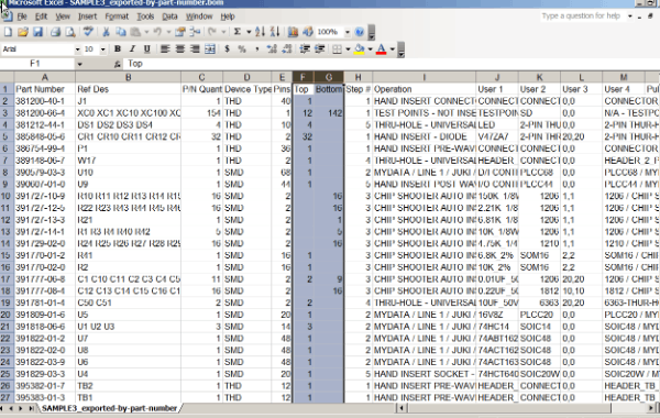
Second, information on how components are mounted onto the board must be conveyed through assembly files. The most critical element is the Bill of Materials (BOM). It is not merely a list of parts but must include accurate manufacturer part numbers, package descriptions, pin numbers, and essential alternative component information. This serves as the sole basis for the procurement team to quickly source materials. The accompanying coordinate files provide the precise location and rotation angle of each component on the PCB, forming the foundational program for driving automated placement machines to achieve accurate placement. Missing or erroneous coordinate files will either halt placement production entirely or result in misaligned components.
Furthermore, while not mandatory, providing design source files or schematics is highly valuable for engineering teams conducting manufacturability analysis and troubleshooting. When design ambiguities arise during production, schematics enable engineers to swiftly grasp circuit intent and make accurate judgments. PCB design source files allow authorized service providers to perform necessary format conversions or optimization analyses, particularly when handling complex packages or high-density layouts, effectively preventing potential production obstacles.
Finally, any special requirements or restrictive documentation should be clearly defined and provided separately. This includes specific soldering process instructions, baking requirements for critical components, test procedures and specifications, and specific acceptance criteria. If the product has compliance requirements, relevant labeling documentation must also be provided. These supplementary documents ensure the service provider not only understands “how to manufacture” but also comprehends “why it is manufactured this way” and “what standards must be met.” This approach enables rapid turnaround without compromising the product's specific performance and reliability requirements.
In conclusion, Quickturn PCB Assembly stands as a defining enabler of modern hardware innovation, transforming the traditional, linear development path into a dynamic and iterative loop. It successfully bridges the critical gap between conceptual design and physical validation by mastering the delicate balance of speed, precision, and quality. From the meticulous preparation of Gerber and BOM files to the strategic application of SMT, through-hole, and specialized soldering techniques, every step is optimized for velocity without compromising integrity. As technology cycles continue to accelerate, this service will only grow in importance, providing the essential agility for developers to test ideas, refine designs, and respond to market demands with confidence and remarkable efficiency. Ultimately, Quickturn PCB Assembly is not merely a manufacturing option; it is a strategic imperative for anyone committed to leading in the relentless race of technological progress.
One-Stop HDI PCB Manufacturer and Its PCB Via Filing Capabilities
If you're looking for turnkey HDI electronics manufacturing services (EMS) from hardware development to PCBA fabrication and box-build assembly, you can work with the one-stop HDI PCBA manufacturer PCBONLINE.
Founded in 1999, PCBONLINE has R&D capabilities for HDI projects and EMS manufacturing capabilities, including via filling for stacked vias. It provides 4-to-64-layer HDI PCB fabrication, assembly, and PCBA box-build assembly. You can order various HDI PCBs from PCBONLINE, such as FR4, polyimide (flexible PCB), polyimide + FR4 (rigid-flex PCB), and PTFE/Rogers (high-frequency PCB).

3000m² of production capacity per day for HDI PCBs with builds of 1+N+1, 2+N+2, 3+N+3,4+N+4, and arbitrary interconnection in any layers.
PCBONLINE has hardware and software R&D capabilities for IoT applications requiring HDI design, including PCBA and enclosures.
We can manufacture complex PCBs with stacker vias, via-in-pad, microvias, inlay boards, heavy copper designs, and hybrid and fine structure lay-ups.
Besides HDI PCB fabrication, we have powerful capabilities in fine-pitch assembly for HDI PCB assembly.
We have rich R&D and manufacturing experience for HDI applications such as FPGA boards.
High-quality HDI PCB and PCBA manufacturing certified with ISO 9001:2015, IATF 16949, RoHS, REACH, UL, and IPC-A-610 Class 2/3.
Here'e the PCB via filing capabilities at PCBONLINEL:
- Micriavia filling with copper: laser via size 0.1-0.125mm, priority 0.1mm
- Finished hole size for via-in-pad filling with resin: 0.1-0.9mm (drill size 0.15-1.0mm), 0.3-0.55mm normal (drill size 0.4-0.65mm)
- Max aspect ratio for via-in-pad filling with resin PCB - 12: 1
- Min resin plugged PCB thickness: 0.2mm
- Max via-filling ith resin PCB thickness: 3.2mm
- Making different hole sizes with via filling in one board: Yes
- Via filling with copper/silver: Yes
If you need HDI PCBAs or any other PCBAs requiring via filling, please send your email to PCBONLINE at info@pcbonline.com. We will provide one-on-one engineering support to you.
Conclusion
Via filling is used for creating stacked vias in HDI PCB fabrication, BGA/CSP/QFN IC packaging, and filling PCB via-in-pad with resin during multilayer PCB fabrication. If you need one-stop electronics manufacturing for your HDI PCBA project, contact the one-stop advanced PCB manufacturer PCBONLINE for high-quality PCBA and box-build solutions tailored to your project's needs.
PCB fabrication at PCBONLINE.pdf


