
This blog systematically outlines the core hardware architecture of network equipment, providing a detailed analysis of the functional characteristics and manufacturing requirements across seven major components—from precision-engineered protective enclosures to highly integrated PCBA assemblies. It covers critical technologies such as power supply redundancy design, intelligent thermal management, and high-speed signal processing, while also delving into the application scenarios for different PCBA types and the stringent standards demanded by their manufacturing processes. This comprehensive perspective offers a thorough understanding of the core technological framework underlying network devices.
Network Equipment Unit
Precision-Protected Enclosure SystemThe enclosure of network equipment serves as its first line of defense against external disturbances, typically constructed from metal to form a robust chassis. It not only effectively shields internal precision components from physical impacts and electromagnetic interference but also provides foundational support for the overall thermal management system through scientifically designed airflow channels, ensuring stable operation under diverse environmental conditions.
Continuous and Stable Power SupplyThe power supply module bears the critical responsibility of converting external AC power into the DC power required by the equipment, serving as the energy source that ensures continuous operation. High-end equipment commonly employs redundant power supply designs. Should one power supply fail, the other immediately takes over, enabling seamless power switching to meet the stringent high-availability requirements of critical operations.
Efficient and Intelligent Thermal ManagementThe cooling system employs a forced airflow channel formed by strategically positioned fans and heat sinks to rapidly dissipate the substantial heat generated by chip operations. An intelligent temperature control system dynamically adjusts fan speeds based on device load, optimizing cooling efficiency while minimizing energy consumption and noise levels to maintain optimal operating temperatures.
Diverse Interface ArrayLine cards and interface modules form the physical gateway connecting the device to external networks, offering multiple access methods including electrical and optical ports. Support for hot-swappable optical modules enables flexible adaptation to different transmission media and speed requirements, providing robust network connectivity and expansion capabilities.
Centralized Command Control HubThe main control board serves as the device's nerve center, equipped with a high-performance processor and running a dedicated network operating system. It not only coordinates system-wide management but also executes core tasks like routing calculations and protocol processing. By generating forwarding rules to guide the data plane's operations, it forms the core of the device's intelligent decision-making.
High-Speed Interconnect Data ChannelsThe switching matrix functions as an internal highway network, providing high-bandwidth, low-latency transmission channels for data exchange between boards. Its backplane switching capacity directly determines the device's overall forwarding performance, serving as critical infrastructure for achieving non-blocking forwarding in modern high-performance network equipment.
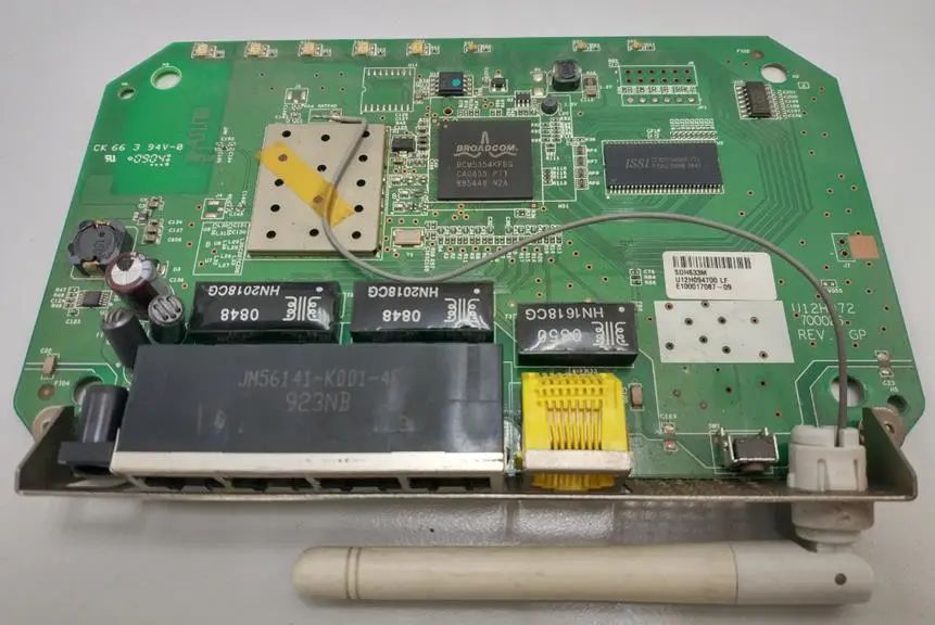
Hardware Foundation for Integrated FunctionalityPrinted circuit board assemblies (PCBAs) form the physical foundation for mounting all electronic components. By highly integrating precision elements like chips, capacitors, and interfaces, they create functional modules that deliver specific capabilities. The quality and design sophistication of these PCBA units directly determine the device's performance and operational reliability, serving as the hardware foundation for all functional implementation.
PCBA Type
Network equipment widely employs various types of PCBA as its core hardware carriers based on functional and performance requirements. Rigid PCBs are the most common foundational type, extensively used in multilayer mainboards for routers, switches, and similar devices due to their high mechanical strength and mature manufacturing processes. When equipment requires processing high-frequency signals (such as 5G base stations), specialized high-frequency PCBs are utilized, employing low-loss materials (e.g., PTFE) to ensure signal integrity. For high-end equipment with limited space and highly complex circuits (like core switches), HDI boards achieve ultra-high-density routing through microvias and blind/buried vias. Flexible PCBs (FPCs) are commonly used for dynamic internal connections, accommodating bending and folding requirements. Rigid-flex boards are employed in specialized three-dimensional structures demanding both stability and flexibility. Additionally, high-power modules (e.g., power supplies and amplifiers) rely on metal substrates (e.g., aluminum substrates) for efficient thermal dissipation. Meanwhile, IC carrier boards housing core chips (e.g., CPUs, NPUs) demand extremely high routing density and signal integrity, requiring manufacturing processes approaching semiconductor-grade precision.
Process Requirements
High-Precision Manufacturing and Assembly Capabilities:
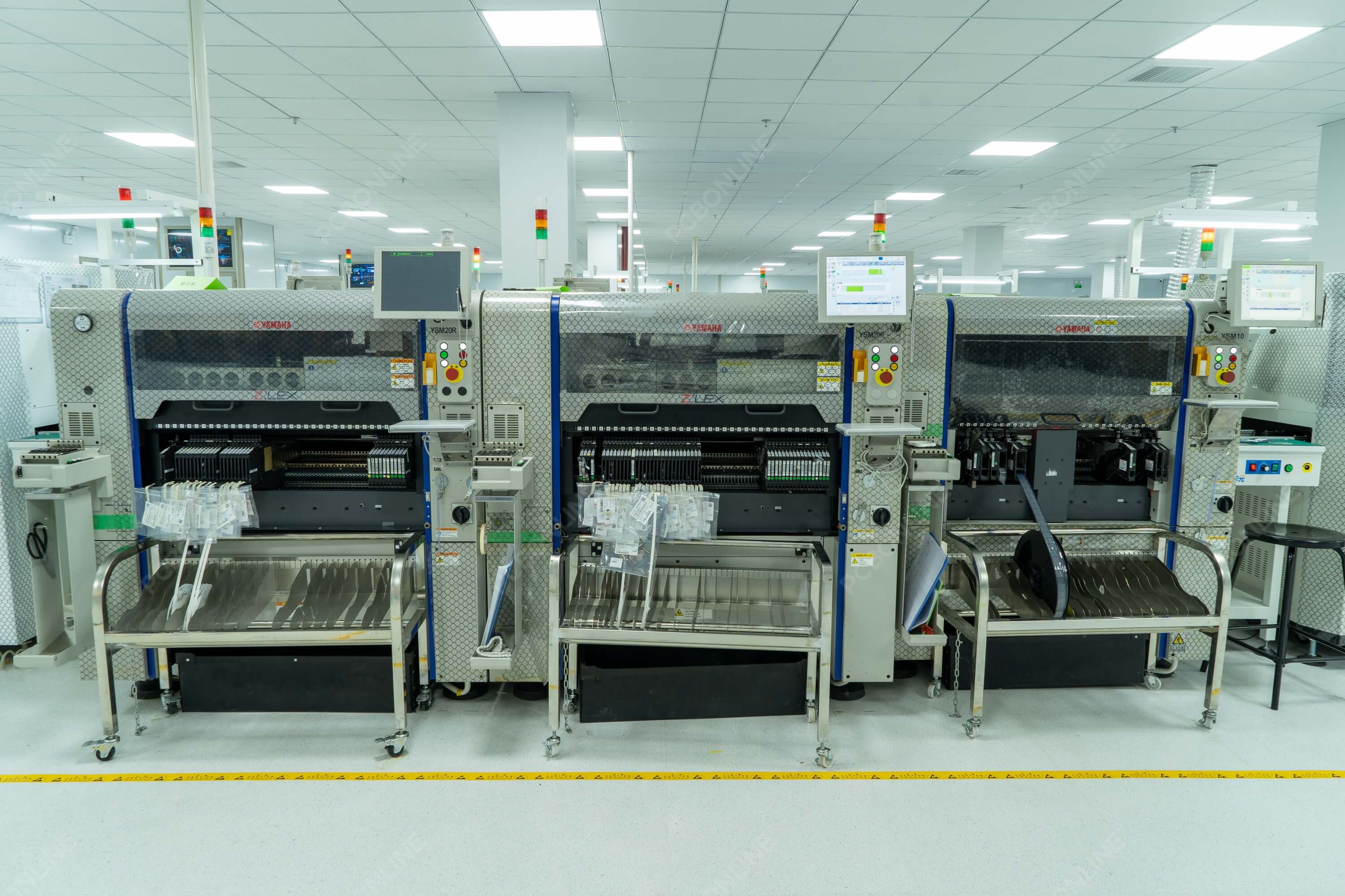
Network equipment demands the utmost reliability from PCBA, which is primarily reflected in its high-precision manufacturing and assembly capabilities. Manufacturers must be equipped with top-tier SMT placement machines and precise process control to handle the increasing number of miniaturized components and high-density packaged chips on boards. This ensures every component is accurately placed and soldered, forming the foundation for all functional stability.
High-Speed Signal Integrity Assurance:
In an era where high-speed signal transmission has become standard, ensuring signal integrity remains a core manufacturing challenge. This demands strict impedance control over PCBs and the skilled application of specialized low-loss materials for circuit fabrication. Such measures guarantee high-frequency signals remain clear and stable during transmission, as even minor deviations can cause significant degradation in device performance.
Advanced Interconnect and Drilling Technologies:
To achieve high-density interconnections in devices, manufacturers must master advanced drilling and lamination techniques. Advanced processes such as laser drilling, via plating, and sequential lamination are critical for manufacturing HDI boards. These technologies enable complex three-dimensional routing within limited spaces, satisfying the dual demands of modern networking equipment for smaller form factors and enhanced performance.
Exceptional Thermal Management Capabilities:
Powerful computing and switching capabilities generate significant heat, necessitating exceptional thermal management throughout the entire manufacturing process. Manufacturers must comprehensively consider heat dissipation solutions during both design and production stages—from employing metal substrates to precisely applying thermal interface materials—to ensure heat generated by high-performance chips is promptly and effectively dissipated, thereby guaranteeing long-term stable device operation.
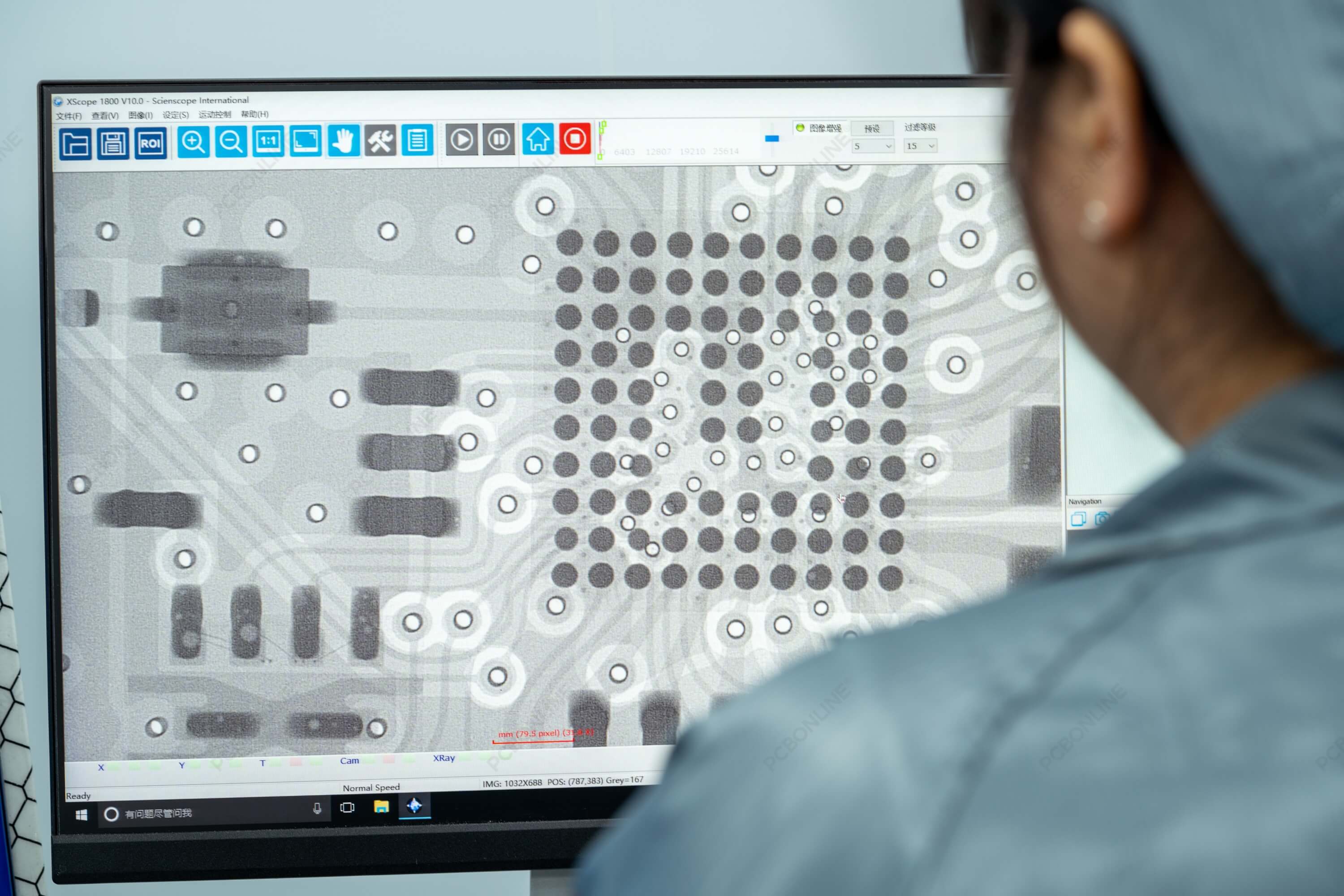
Comprehensive Testing and Inspection Capabilities:
Comprehensive testing and inspection serve as the most critical quality gate before products leave the factory. From initial in-line testing to functional testing simulating real-world environments, and extending to X-ray inspection targeting hidden solder joints, a multi-tiered, all-encompassing testing system is the sole means to screen out defects and ensure every PCBA meets design specifications 100%.
Reliability Design and Certification:
Network equipment typically requires round-the-clock operation without interruption, necessitating designs that adhere to high reliability standards. Manufacturers often subject these devices to environmental stress screening and aging tests exceeding conventional requirements, simulating various harsh operating conditions. This ensures products can withstand the rigors of long-term operation after delivery, minimizing field failure rates to the greatest extent possible.
Clean and Eco-Friendly Manufacturing:
Highly clean and eco-friendly manufacturing is an often overlooked yet critical aspect. Even minute contaminants can compromise the electrical performance of high-frequency circuits, necessitating extremely stringent production environments and cleaning procedures. Simultaneously, the entire process must comply with environmental regulations by utilizing green materials and processes—a requirement not only for regulatory compliance but also as a demonstration of corporate social responsibility.
Network equipment achieves high performance and reliability through the deep integration of precision hardware and intelligent software. It comprises a physical enclosure system for protection, power modules as the energy foundation, thermal management systems for temperature control, interface arrays as connectivity gateways, control hubs as decision centers, data channels as transmission lifelines, and PCBA as functional carriers—collectively forming a robust network infrastructure. Manufacturing processes must meet seven core requirements: high-precision placement, signal integrity control, advanced interconnect technologies, optimized thermal management, comprehensive testing and certification, reliability design, and clean production. This ensures sustained, stable operation of equipment in complex environments.
One-Stop HDI PCB Manufacturer and Its PCB Via Filing Capabilities
If you're looking for turnkey HDI electronics manufacturing services (EMS) from hardware development to PCBA fabrication and box-build assembly, you can work with the one-stop HDI PCBA manufacturer PCBONLINE.
Founded in 1999, PCBONLINE has R&D capabilities for HDI projects and EMS manufacturing capabilities, including via filling for stacked vias. It provides 4-to-64-layer HDI PCB fabrication, assembly, and PCBA box-build assembly. You can order various HDI PCBs from PCBONLINE, such as FR4, polyimide (flexible PCB), polyimide + FR4 (rigid-flex PCB), and PTFE/Rogers (high-frequency PCB).

3000m² of production capacity per day for HDI PCBs with builds of 1+N+1, 2+N+2, 3+N+3,4+N+4, and arbitrary interconnection in any layers.
PCBONLINE has hardware and software R&D capabilities for IoT applications requiring HDI design, including PCBA and enclosures.
We can manufacture complex PCBs with stacker vias, via-in-pad, microvias, inlay boards, heavy copper designs, and hybrid and fine structure lay-ups.
Besides HDI PCB fabrication, we have powerful capabilities in fine-pitch assembly for HDI PCB assembly.
We have rich R&D and manufacturing experience for HDI applications such as FPGA boards.
High-quality HDI PCB and PCBA manufacturing certified with ISO 9001:2015, IATF 16949, RoHS, REACH, UL, and IPC-A-610 Class 2/3.
Here'e the PCB via filing capabilities at PCBONLINEL:
- Micriavia filling with copper: laser via size 0.1-0.125mm, priority 0.1mm
- Finished hole size for via-in-pad filling with resin: 0.1-0.9mm (drill size 0.15-1.0mm), 0.3-0.55mm normal (drill size 0.4-0.65mm)
- Max aspect ratio for via-in-pad filling with resin PCB - 12: 1
- Min resin plugged PCB thickness: 0.2mm
- Max via-filling ith resin PCB thickness: 3.2mm
- Making different hole sizes with via filling in one board: Yes
- Via filling with copper/silver: Yes
If you need HDI PCBAs or any other PCBAs requiring via filling, please send your email to PCBONLINE at info@pcbonline.com. We will provide one-on-one engineering support to you.
Conclusion
Via filling is used for creating stacked vias in HDI PCB fabrication, BGA/CSP/QFN IC packaging, and filling PCB via-in-pad with resin during multilayer PCB fabrication. If you need one-stop electronics manufacturing for your HDI PCBA project, contact the one-stop advanced PCB manufacturer PCBONLINE for high-quality PCBA and box-build solutions tailored to your project's needs.
PCB fabrication at PCBONLINE.pdf


