
Industrial-grade PCBs (printed circuit boards) are core components of modern industrial systems and are widely used in key areas such as manufacturing, automotive, energy, and healthcare. Their high reliability, precision, and durability directly determine the performance and safety of equipment. With the rapid development of industrial automation and the Internet of Things (IoT), the demand for multilayer PCBs (such as 18 layers and above) has skyrocketed, and their manufacturing processes and testing standards have become increasingly stringent.
In this article:
Part 1. The Critical Role of Industrial PCBs Part 2. Advanced Manufacturing Processes Part 3. Quality Control and TestingThe Critical Role of Industrial PCBs
Industrial PCBs serve as the nervous system for mission-critical applications across multiple sectors. In manufacturing plants, they control robotic arms and assembly lines with precision timing measured in milliseconds. Automotive systems rely on them for engine control units (ECUs) that must function flawlessly from -40°C to 150°C. Energy infrastructure depends on industrial-grade PCBs to manage power distribution in solar inverters and smart grids. Even healthcare institutions trust these robust circuit boards to operate MRI machines and life-support equipment where failure is not an option.
The growing demand for industrial automation and IoT connectivity has dramatically increased the need for specialized PCB solutions. According to industry reports, the global PCB market reached $735.65 billion in 2024, with industrial applications representing a significant and growing segment. Particularly in sectors like AI servers and high-performance computing, multilayer PCBs (18 layers and above) saw a 40.2% year-over-year growth in 2024—far outpacing the overall PCB market growth of 5.8%
Advanced Manufacturing Processes
Industrial PCB production involves sophisticated manufacturing techniques that go far beyond standard PCB fabrication. The process begins with high-performance substrate materials like FR-4 with high glass transition temperatures (Tg 170+), metal-core boards for thermal management, or even innovative glass substrates for RF and optoelectronic applications. These specialized materials provide the foundation for circuits that must maintain signal integrity in electrically noisy industrial environments.
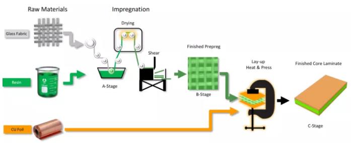
One of the most critical stages in industrial PCB manufacturing is the lamination process for multilayer boards. Companies like PCBONLINE have developed patented thick-copper lamination techniques that address challenges like resin bleed and dust contamination during routing operations. Their optimized process uses CCD alignment cameras and specialized routing parameters to achieve precision bonding of prepreg materials. Such innovations are essential for producing the high-current power distribution layers found in industrial motor drives and power converters.
Drilling technology represents another area where industrial requirements push the boundaries of PCB manufacturing. As boards grow more complex—with layer counts exceeding 20 in some server applications—the need for precise microvias (often below 100μm diameter) has driven adoption of advanced laser drilling systems. Ultrafast femtosecond and picosecond lasers now enable clean, microcrack-free holes in brittle materials like glass substrates, opening new possibilities for high-frequency and optoelectronic integration.
PCB Motor Typical Problem Case Analysis and Solutions
The Rigorous Testing Regimen of Industrial PCBsThe journey of an industrial PCB through quality assurance begins long before the final product is assembled. From raw material inspection to environmental stress testing, manufacturers employ a multi-layered approach to detect and eliminate potential failures.
One of the most critical early-stage tests is Automated Optical Inspection (AOI), where high-resolution cameras scan the PCB for defects such as incorrect trace widths, missing solder mask, or misaligned components. Advanced AOI systems now incorporate AI-driven image recognition, allowing them to learn from past defects and improve detection accuracy over time.
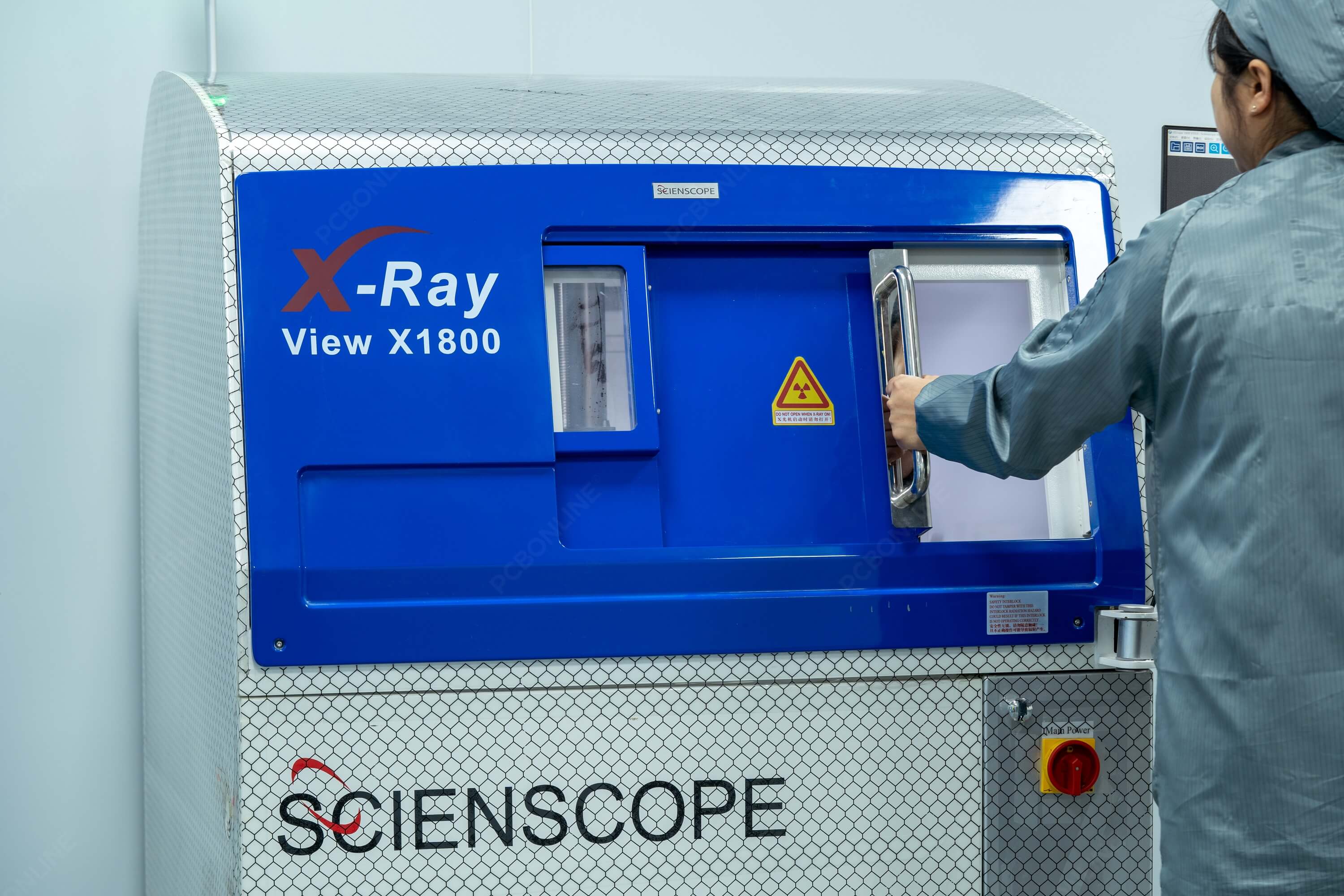
For multilayer PCBs, X-ray inspection (AXI) plays a crucial role in verifying internal layer alignment and detecting hidden defects like voids in vias or delamination between layers. This is particularly important in high-reliability applications such as aerospace or medical devices, where internal flaws could lead to catastrophic failures.
Once the PCB passes visual inspections, it undergoes electrical testing to confirm that all circuits function as designed. Flying Probe Testing (FPT) is commonly used for prototypes and low-volume production, where robotic probes check each net for continuity and isolation. For high-volume manufacturing, In-Circuit Testing (ICT) provides faster validation by using a bed-of-nails fixture to test multiple points simultaneously.
However, industrial PCBs often require more than just basic connectivity checks. Impedance testing ensures signal integrity in high-speed designs, while high-voltage testing verifies insulation resistance in power electronics. Some manufacturers even perform burn-in testing, where boards are operated at elevated temperatures for extended periods to weed out early-life failures.
Environmental Stress Testing: Simulating Years of Use in HoursPerhaps the most defining characteristic of industrial PCB testing is its focus on environmental resilience. Unlike consumer-grade boards, industrial PCBs must endure extreme temperatures, humidity, vibration, and chemical exposure. To validate their durability, manufacturers subject samples to accelerated life testing (ALT).
One common method is thermal cycling, where boards repeatedly transition between extreme cold (-55°C) and heat (125°C) to simulate years of thermal stress. Vibration and shock testing replicate the mechanical stresses encountered in automotive or heavy machinery applications. Additionally, salt spray testing evaluates corrosion resistance—a critical factor for PCBs used in marine or outdoor industrial equipment.
The Role of Data Analytics in Modern PCB QCLeading manufacturers are now integrating real-time data analytics into their quality control processes. By collecting data from AOI, electrical tests, and environmental trials, they can identify trends and predict potential failure modes before they occur. Some factories even employ digital twin technology, where virtual models of PCBs are tested under simulated conditions to optimize designs before physical production begins.
Industrial PCBs serve as the “invisible cornerstone” supporting the intelligentization and automation of modern industry. Their manufacturing process not only relies on advanced materials and processes (such as thick copper lamination and laser micro-hole drilling) but also requires multi-level quality inspections (such as AOI, AXI, and flying probe testing) and extreme environmental stress testing (such as high-low temperature cycling and vibration/shock testing). With the application of data analysis and digital twin technology, the reliability of industrial PCBs has been further enhanced, providing indispensable hardware support for critical fields such as AI servers, smart grids, and medical devices.
One-Stop HDI PCB Manufacturer and Its PCB Via Filing Capabilities
If you're looking for turnkey HDI electronics manufacturing services (EMS) from hardware development to PCBA fabrication and box-build assembly, you can work with the one-stop HDI PCBA manufacturer PCBONLINE.
Founded in 1999, PCBONLINE has R&D capabilities for HDI projects and EMS manufacturing capabilities, including via filling for stacked vias. It provides 4-to-64-layer HDI PCB fabrication, assembly, and PCBA box-build assembly. You can order various HDI PCBs from PCBONLINE, such as FR4, polyimide (flexible PCB), polyimide + FR4 (rigid-flex PCB), and PTFE/Rogers (high-frequency PCB).

3000m² of production capacity per day for HDI PCBs with builds of 1+N+1, 2+N+2, 3+N+3,4+N+4, and arbitrary interconnection in any layers.
PCBONLINE has hardware and software R&D capabilities for IoT applications requiring HDI design, including PCBA and enclosures.
We can manufacture complex PCBs with stacker vias, via-in-pad, microvias, inlay boards, heavy copper designs, and hybrid and fine structure lay-ups.
Besides HDI PCB fabrication, we have powerful capabilities in fine-pitch assembly for HDI PCB assembly.
We have rich R&D and manufacturing experience for HDI applications such as FPGA boards.
High-quality HDI PCB and PCBA manufacturing certified with ISO 9001:2015, IATF 16949, RoHS, REACH, UL, and IPC-A-610 Class 2/3.
Here'e the PCB via filing capabilities at PCBONLINEL:
- Micriavia filling with copper: laser via size 0.1-0.125mm, priority 0.1mm
- Finished hole size for via-in-pad filling with resin: 0.1-0.9mm (drill size 0.15-1.0mm), 0.3-0.55mm normal (drill size 0.4-0.65mm)
- Max aspect ratio for via-in-pad filling with resin PCB - 12: 1
- Min resin plugged PCB thickness: 0.2mm
- Max via-filling ith resin PCB thickness: 3.2mm
- Making different hole sizes with via filling in one board: Yes
- Via filling with copper/silver: Yes
If you need HDI PCBAs or any other PCBAs requiring via filling, please send your email to PCBONLINE at info@pcbonline.com. We will provide one-on-one engineering support to you.
Conclusion
Via filling is used for creating stacked vias in HDI PCB fabrication, BGA/CSP/QFN IC packaging, and filling PCB via-in-pad with resin during multilayer PCB fabrication. If you need one-stop electronics manufacturing for your HDI PCBA project, contact the one-stop advanced PCB manufacturer PCBONLINE for high-quality PCBA and box-build solutions tailored to your project's needs.
PCB fabrication at PCBONLINE.pdf


