
When the EU RoHS Directive (Restriction of the Use of Certain Hazardous Substances in Electrical and Electronic Equipment) approached its effective date in 2006, the entire electronics manufacturing industry chain was caught in a data storm. Original equipment manufacturers (OEMs), suppliers and manufacturers suddenly faced a huge challenge: how to efficiently collect, manage and exchange compliance information on hazardous substances in massive amounts of materials? At the time, each company used custom forms and reporting formats, resulting in confusing data, high exchange costs and frequent errors. It was against this background that the IPC-1752 standard came into being.
In this article:
Part 1. What is IPC-1752A Part 2. Six-tier Reporting System: Flexibly Responding to Compliance Complexity Part 3. Efficiency Benefit: Streamlining Global Supply Chain Collaboration Part 4. The long-term Value of Green ComplianceWhat is IPC-1752A
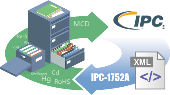
IPC-1752A is a Materials Declaration Management standard developed by the Internet Electronics Industry Association (IPC) of the United States. It is mainly used to regulate the exchange of environmental compliance data on product material components in the electronic product supply chain. It provides a unified material component declaration format for upstream and downstream companies in the supply chain (such as raw material suppliers, component factories, assembly plants, etc.), ensures efficient data transmission, and supports compliance requirements of environmental regulations (such as the EU RoHS Directive). Compared with the traditional material declaration, which has problems such as confusing formats and low efficiency, IPC-1752A simplifies the process through standardized electronic forms (PDF/XML format) to reduce corporate compliance costs.
Six-tier Reporting System: Flexibly Responding to Compliance Complexity
Level 1 and Level 2: Focus on basic RoHS compliance (yes/no), where Level 2 additionally includes manufacturing process information, suitable for general components and simple products.
Level 3 and Level 4: Introduce JIG (Joint Industry Guide) classification, disclose material information at the part level, and Level 4 also adds manufacturing process data, suitable for materials requiring medium transparency.
Level 5 and Level 6: The most stringent requirements - all restricted substances (including JIG and other substances) must be disclosed at the homogeneous material level, and Level 6 further includes manufacturing process tracking. This is particularly important for high-risk industries such as medical devices and automotive electronics.
This design allows suppliers to flexibly choose the reporting depth based on customer requirements or product risk level, avoiding the additional costs caused by a "one-size-fits-all" approach.
Efficiency Benefit: Streamlining Global Supply Chain Collaboration
Before the implementation of IPC-1752, a manufacturer may have to deal with hundreds of different declaration forms from suppliers, and manual verification is time-consuming and prone to errors.
The standard completely optimizes this process through two mechanisms:
Standardized data exchange: All declarations use a unified XML structure to generate PDF or electronic forms, supporting automated data reading and integration (such as PLM systems).
Dual-path collaboration model: supports both "request-response" (customers actively request data) and "publish" (suppliers actively push updates) modes to adapt to diverse supply chain relationships
The long-term Value of Green Compliance
Although the initial impetus for IPC-1752 was to respond to the RoHS directive, its influence has long surpassed a single regulation. It has become the underlying data bridge for responding to global environmental regulations (such as REACH and WEEE). Once an enterprise establishes an IPC-1752 compliance system, it can quickly adapt to the new regulations - for example, directly meet the needs of the EU SCIP database (Substances of High Concern Notification) through Level 5 declaration.
More importantly, IPC-1752 accelerates the transformation of the electronics industry to a circular economy by promoting supply chain transparency. Manufacturers can optimize material selection based on declaration data (such as eliminating PFAS-containing coatings), and recyclers can also accurately disassemble high-risk components. This transition from "compliance defense" to "sustainable design" is the biggest legacy of IPC-1752 to the industry.
Nearly two decades later, IPC-1752 remains the cornerstone of green compliance in the global electronics manufacturing industry. Its success proves a truth: when addressing systemic challenges, open and collaborative standards are often more viable than closed solutions. As low-carbon manufacturing and ESG (environmental, social and governance) requirements become new focuses, IPC-1752's data framework is paving the way for the next generation of standards (such as carbon footprint tracking). For companies that are still groping in the labyrinth of compliance, embracing this standard is not only a shield to avoid risks, but also the key to winning the global market.
One-Stop HDI PCB Manufacturer and Its PCB Via Filing Capabilities
If you're looking for turnkey HDI electronics manufacturing services (EMS) from hardware development to PCBA fabrication and box-build assembly, you can work with the one-stop HDI PCBA manufacturer PCBONLINE.
Founded in 1999, PCBONLINE has R&D capabilities for HDI projects and EMS manufacturing capabilities, including via filling for stacked vias. It provides 4-to-64-layer HDI PCB fabrication, assembly, and PCBA box-build assembly. You can order various HDI PCBs from PCBONLINE, such as FR4, polyimide (flexible PCB), polyimide + FR4 (rigid-flex PCB), and PTFE/Rogers (high-frequency PCB).

3000m² of production capacity per day for HDI PCBs with builds of 1+N+1, 2+N+2, 3+N+3,4+N+4, and arbitrary interconnection in any layers.
PCBONLINE has hardware and software R&D capabilities for IoT applications requiring HDI design, including PCBA and enclosures.
We can manufacture complex PCBs with stacker vias, via-in-pad, microvias, inlay boards, heavy copper designs, and hybrid and fine structure lay-ups.
Besides HDI PCB fabrication, we have powerful capabilities in fine-pitch assembly for HDI PCB assembly.
We have rich R&D and manufacturing experience for HDI applications such as FPGA boards.
High-quality HDI PCB and PCBA manufacturing certified with ISO 9001:2015, IATF 16949, RoHS, REACH, UL, and IPC-A-610 Class 2/3.
Here'e the PCB via filing capabilities at PCBONLINEL:
- Micriavia filling with copper: laser via size 0.1-0.125mm, priority 0.1mm
- Finished hole size for via-in-pad filling with resin: 0.1-0.9mm (drill size 0.15-1.0mm), 0.3-0.55mm normal (drill size 0.4-0.65mm)
- Max aspect ratio for via-in-pad filling with resin PCB - 12: 1
- Min resin plugged PCB thickness: 0.2mm
- Max via-filling ith resin PCB thickness: 3.2mm
- Making different hole sizes with via filling in one board: Yes
- Via filling with copper/silver: Yes
If you need HDI PCBAs or any other PCBAs requiring via filling, please send your email to PCBONLINE at info@pcbonline.com. We will provide one-on-one engineering support to you.
Conclusion
Via filling is used for creating stacked vias in HDI PCB fabrication, BGA/CSP/QFN IC packaging, and filling PCB via-in-pad with resin during multilayer PCB fabrication. If you need one-stop electronics manufacturing for your HDI PCBA project, contact the one-stop advanced PCB manufacturer PCBONLINE for high-quality PCBA and box-build solutions tailored to your project's needs.
PCB fabrication at PCBONLINE.pdf


