
In modern power electronics, industrial control, medical devices, and new energy systems, high voltage PCB design has become a core skill that electronic engineers must master. Unlike conventional low-voltage circuit board design, high voltage PCBs face a series of unique challenges, including electrical breakdown, arc discharge, creepage distance control, thermal management, and electromagnetic compatibility. This article will delve into the engineering practices of high voltage PCB design from three key technical dimensions: materials science, layout planning and safety standards, and manufacturing and testing. It will provide engineers with directly applicable professional solutions, focusing entirely on technical implementation while avoiding market analysis to ensure professional depth and practical value.
In this article:
Part 1. Materials Science for High Voltage PCBs Part 2. Safety Spacing, Electric Field Control, and Thermal Management Part 3. High Voltage PCB Manufacturing Processes and Testing VerificationMaterials Science for High Voltage PCBs
Analysis of Substrate Material Dielectric Properties and Breakdown Strength
The primary consideration in high voltage PCB design is the dielectric performance of the substrate material. FR-4, as the most common PCB substrate, has a typical breakdown strength of about 20-40 kV/mm (depending on the specific formulation and thickness). It may face challenges in applications exceeding 15kV or involving high-frequency, high-voltage pulses. For higher voltage requirements, engineers should consider:
Specialty Epoxy-based Materials: Such as Isola's IS-410 and Panasonic's R-1755V series, with breakdown strengths reaching 50-80 kV/mm while maintaining good machinability.
Polyimide (PI) Materials: Excellent performance in high-temperature, high-voltage environments, with breakdown strengths exceeding 100 kV/mm and glass transition temperatures (Tg) above 250°C, making them particularly suitable for aerospace and oil & gas exploration equipment.
Polytetrafluoroethylene (PTFE) based materials: Stable dielectric constant (typically 2.0-2.8) and extremely low loss factor (0.0009-0.002), suitable for high-frequency, high-voltage applications like RF power supplies and radar systems.
Ceramic-filled Substrates: Such as insulated metal substrates (IMS) and direct bonded copper (DBC) ceramic substrates, offering excellent thermal conductivity (1-24 W/mK) and high voltage tolerance, suitable for high-power IGBT modules and solid-state transformers.
High Voltage Considerations for Copper Foil Thickness and Surface Finish
Conductor design in high voltage PCBs must consider current density and surface discharge characteristics:
Copper Foil Thickness Selection: High-voltage, high-current paths should use 2-6 oz/ft² (70-210 μm) thick copper foil to reduce temperature rise and electromigration risks. For extreme applications, plating techniques can be used to locally increase thickness to 400 μm in critical areas.
Surface Finish Processes:
- Immersion Silver: Provides a flat surface, reducing corona discharge, but generally has limited long-term voltage resistance.
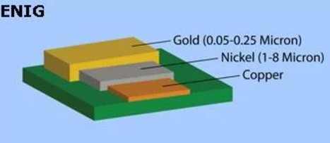
- ENIG (Electroless Nickel Immersion Gold): Excellent surface flatness and oxidation resistance, suitable for high-voltage connector areas.
- OSP (Organic Solderability Preservative): Lower cost, but limited tolerance for repeated soldering.
- Hard Gold Plating: Suitable for high-voltage sliding contacts and connectors, offering excellent wear resistance.
Dielectric Stack-up Design for Multilayer Boards
High voltage multilayer PCBs require careful dielectric layer stack-up design:
Interlayer Dielectric Thickness Calculation: Based on the peak operating voltage and safety requirements, the interlayer dielectric thickness should satisfy:
Thickness (mm) ≥ (Peak Operating Voltage × Safety Factor) / Material Breakdown Strength
The safety factor is typically 1.5-3.0, depending on the safety classification of the application environment.
Gradient Dielectric Constant Design: For mixed-signal high-voltage boards, gradient dielectric constant materials can be used, employing high dielectric strength materials (e.g., Rogers RO4350B) in high-voltage areas and low-loss materials (e.g., Rogers RO4003C) in high-speed areas.
Prepreg Selection: High-voltage applications should use prepregs with high resin content (e.g., type 1080 rather than 7628) to ensure complete filling of interlayer voids and eliminate partial discharge risks.
|
Parameter
|
General Requirement / Value
|
Key Limitation / Challenge
|
|
Laser Via Diameter
|
0.1mm (typical)
|
Range: 0.075-0.15mm. Must maintain low aspect ratio (≤1:1).
|
|
Trace/Space
|
≥3.5/3.5 mil (recommended)
|
Approaching 2.7/2.7 mil significantly increases cost/difficulty.
|
|
Annular Ring
|
≥0.15mm
|
Critical for blind/buried via reliability.
|
|
Via-to-Via Spacing
|
≥0.24mm
|
A major constraint in ultra-high-density BGA fanout.
|
|
HDI Sequence
|
1+N+1, 2+N+2, etc.
|
Higher sequence = more lamination/drilling cycles, exponentially increasing cost.
|
Safety Spacing, Electric Field Control, and Thermal Management
Creepage and Clearance Calculations Based on Standards
Creepage distance (along the surface) and clearance (shortest air path) are core parameters in high voltage PCB design:
International Standard References:
- IPC-2221B: Generic Standard on Printed Board Design
- IEC 60950-1: Safety of Information Technology Equipment
- IEC 60664-1: Insulation Coordination for Equipment within Low-Voltage Systems
- UL 60950: Safety Standards for Specific Industries
Pollution Degree Consideration: Designs must account for the pollution degree (levels 1-4) of the operating environment, which significantly impacts creepage distance requirements. For example, under Pollution Degree 2 (general industrial environment), for AC 1000V RMS (peak ~1414V), the creepage requirement for Material Group I is 10mm, while under Pollution Degree 3 it may increase to 16mm.
Calculation Example:
For a DC 10kV application, Pollution Degree 2, using Material Group I (CTI ≥ 600):
Basic Clearance: According to IEC 60664-1 Table F.2, Overvoltage Category III, at least 25mm for 10kV.
Creepage Distance: According to Table F.4, at least 125mm for 10kV.
Actual design must also consider the altitude correction factor (increase required for >2000m) and pulse voltage waveform factors.
Electric Field Control and Edge Optimization Techniques
Conductor Edge Treatment:
- Use rounded corners or chamfers instead of right angles (to reduce electric field concentration).
- Implement tapered transitions for high-voltage trace widths to avoid abrupt changes.
- Apply additional plating at critical edges to form a uniform electric field distribution.
Guard Ring Design:
Place grounded guard rings around high-voltage areas, with a width of at least 1mm, spaced from the high-voltage conductor at 50-70% of the safety distance, effectively controlling electric field divergence.
Dielectric Slot Application:
Create slots between areas of extremely high potential difference, forcing current to flow along a longer surface path, thereby increasing the effective creepage distance. Slot width is typically 1-3mm, with depth ensuring sufficient mechanical strength.
Thermal Management and Partial Discharge Suppression
Thermal Design for High Voltage Areas:
- High-voltage, high-current paths should be kept away from thermally sensitive components.
- Implement thermal via arrays under power devices (diameter 0.3-0.5mm, pitch 1.5-2mm).
- Use thermal simulation to identify hotspots; integrate metal cores or heat sinks if necessary.
Enhancing Partial Discharge (PD) Inception Voltage:
- Use smooth transitions for all high-voltage connection points to avoid spikes and burrs.
- Apply vacuum impregnation treatment to fill potential air gaps.
- Use potting compounds with matched dielectric constants (e.g., silicone gel) to protect critical areas.
- Perform partial discharge testing after PCB manufacturing to ensure the inception voltage is above 1.5 times the operating voltage.
Zoning Layout Strategy:
Divide the PCB into high-voltage, low-voltage, and interface zones, with isolation gaps of at least 5mm between zones. Use optocouplers, capacitive coupling, or transformers in the interface zone for signal and power transfer.
High Voltage PCB Manufacturing Processes and Testing Verification
Specialized Manufacturing Processes and Techniques
High Voltage Copper Foil Treatment:
- Use reverse-treated foil (RTF) or very low profile (VLP) copper foil to reduce copper roughness and improve surface flatness.
- Perform thorough micro-etching before plating to ensure copper surface cleanliness.
- Implement pulse plating to obtain dense and uniform copper layers.
Drilling and Hole Wall Quality:
- Use high-quality carbide drill bits to minimize hole wall roughness (target Ra < 32μm).
- Plate through-holes twice or three times to ensure hole wall copper thickness ≥ 25μm.
- Use resin plugging techniques to fill unnecessary voids, preventing surface tracking.
Solder Mask Application:

- Choose high voltage resistant solder mask materials (e.g., Taiyo PSR-4000 series).
- Ensure solder mask fully covers high-voltage trace edges, with an overhang of at least 0.2mm.
- Maintain uniform solder mask thickness without thin spots or bubbles (target thickness 20-30μm).
Quality Control and Electrical Testing
Raw Material Incoming Inspection:
- Substrate breakdown strength test (ASTM D149).
- Copper foil roughness measurement (contact profilometer).
- Dielectric constant and loss factor verification (resonant cavity or parallel plate method).
In-Process Quality Control Points:
-
After Inner Layer Etching: Inspect line edge smoothness, ensuring no burrs or notches.
-
After Lamination: Perform ultrasonic scanning to detect interlayer delamination and voids.
-
After Drilling: Microscope inspection (100-200x) of hole wall quality.
-
After Plating: Copper thickness measurement (microsection analysis).
High Voltage Electrical Testing Protocol:
Hi-Pot (Withstand Voltage) Test:
Test Voltage = Rated Working Voltage × 2 + 1000V (or per product standard)
Test Duration: Typically 60 seconds
Leakage Current Threshold: Typically < 1mA
Test Points: All high-voltage nets vs. low-voltage nets and ground.
Insulation Resistance Test:
- Test Voltage: 500V DC or 1000V DC (depending on rated voltage).
- Requirement: Typically > 1000 MΩ (> 100 MΩ after humidity test).
- Test Points: Between adjacent high-voltage traces; between high-voltage and ground.
Partial Discharge Test:
- Test Equipment: PD test system compliant with IEC 60270.
- Test Voltage: Gradually increased to 1.5-2 times the working voltage.
- Acceptance Criterion: PD magnitude < 5 pC at 1.1 times the working voltage.
Environmental Adaptability Verification and Lifetime Assessment
Environmental Test Sequence:
-
Thermal Cycling Test: -40°C to +125°C, 1000 cycles, with no degradation in withstand voltage performance after testing.
-
Damp Heat Aging: 85°C/85% RH, 1000 hours, with insulation resistance retention > 80%.
-
High Voltage Endurance Test: Continuous operation at 1.2 times rated voltage for 1000 hours, with no performance degradation.
Key Performance Monitoring Parameters:
- Trend of Surface Insulation Resistance (SIR).
- Stability of Dissipation Factor (tan δ).
- Changes in Partial Discharge Inception and Extinction Voltages.
- Stability of Thermal Resistance (Rth).
Failure Analysis Techniques:
When tests fail, the following should be employed:
-
Thermal Imaging Analysis: Locate localized hot spots.
-
Scanning Electron Microscopy (SEM): Analyze the microstructure of breakdown paths.
-
Energy Dispersive X-ray Spectroscopy (EDS): Identify contaminant composition.
-
Focused Ion Beam (FIB) Sectioning: Observe the 3D structure of internal defects.
High voltage PCB design is a comprehensive engineering discipline that integrates materials science, electric field theory, thermodynamics, and manufacturing processes. Successful high voltage PCB design requires not only strict adherence to international safety standards but also a deep understanding of material properties, electric field behavior, and failure mechanisms. From the selection of specialty substrates to precise layout planning, from stringent manufacturing process control to comprehensive electrical testing, each stage demands rigorous calculation and verification by the engineer.
One-Stop HDI PCB Manufacturer and Its PCB Via Filing Capabilities
If you're looking for turnkey HDI electronics manufacturing services (EMS) from hardware development to PCBA fabrication and box-build assembly, you can work with the one-stop HDI PCBA manufacturer PCBONLINE.
Founded in 1999, PCBONLINE has R&D capabilities for HDI projects and EMS manufacturing capabilities, including via filling for stacked vias. It provides 4-to-64-layer HDI PCB fabrication, assembly, and PCBA box-build assembly. You can order various HDI PCBs from PCBONLINE, such as FR4, polyimide (flexible PCB), polyimide + FR4 (rigid-flex PCB), and PTFE/Rogers (high-frequency PCB).

3000m² of production capacity per day for HDI PCBs with builds of 1+N+1, 2+N+2, 3+N+3,4+N+4, and arbitrary interconnection in any layers.
PCBONLINE has hardware and software R&D capabilities for IoT applications requiring HDI design, including PCBA and enclosures.
We can manufacture complex PCBs with stacker vias, via-in-pad, microvias, inlay boards, heavy copper designs, and hybrid and fine structure lay-ups.
Besides HDI PCB fabrication, we have powerful capabilities in fine-pitch assembly for HDI PCB assembly.
We have rich R&D and manufacturing experience for HDI applications such as FPGA boards.
High-quality HDI PCB and PCBA manufacturing certified with ISO 9001:2015, IATF 16949, RoHS, REACH, UL, and IPC-A-610 Class 2/3.
Here'e the PCB via filing capabilities at PCBONLINEL:
- Micriavia filling with copper: laser via size 0.1-0.125mm, priority 0.1mm
- Finished hole size for via-in-pad filling with resin: 0.1-0.9mm (drill size 0.15-1.0mm), 0.3-0.55mm normal (drill size 0.4-0.65mm)
- Max aspect ratio for via-in-pad filling with resin PCB - 12: 1
- Min resin plugged PCB thickness: 0.2mm
- Max via-filling ith resin PCB thickness: 3.2mm
- Making different hole sizes with via filling in one board: Yes
- Via filling with copper/silver: Yes
If you need HDI PCBAs or any other PCBAs requiring via filling, please send your email to PCBONLINE at info@pcbonline.com. We will provide one-on-one engineering support to you.
Conclusion
Via filling is used for creating stacked vias in HDI PCB fabrication, BGA/CSP/QFN IC packaging, and filling PCB via-in-pad with resin during multilayer PCB fabrication. If you need one-stop electronics manufacturing for your HDI PCBA project, contact the one-stop advanced PCB manufacturer PCBONLINE for high-quality PCBA and box-build solutions tailored to your project's needs.
PCB fabrication at PCBONLINE.pdf


