
Have you ever wondered how smart devices achieve hardware-level flexibility when they need to rapidly adapt to new features and process massive amounts of data? This article will provide a deep dive into the core technology of FPGAs, revealing the unique appeal of these programmable chips: how they break free from the constraints of traditional hardware, enabling astonishing customization and parallel processing capabilities, and complementing the familiar CPUs and GPUs.
In this article:
Part 1. What is FPGA and How Do Programmable Chips Drive Innovation Part 2. Core Advantages of FPGAs Part 3. Similarities and Differences between FPGAs and CPUs/GPUs Part 4. FPGA ApplicationsWhat is FPGA and How Do Programmable Chips Drive Innovation
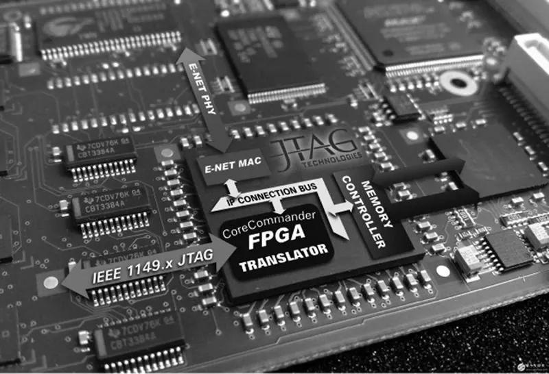
In the rapidly evolving world of technology, FPGAs (Field-Programmable Gate Arrays) are playing an increasingly important role. Unlike traditional fixed-function chips, FPGAs are highly flexible semiconductor devices that allow users to program and configure them at the hardware level, enabling customized circuit functionality. This unique "plasticity" has made FPGAs an indispensable technological cornerstone in numerous fields, from efficient data center operations to precise control of autonomous driving to intelligent diagnostics in medical devices. Their ubiquitous presence provides powerful hardware support for the advancement of modern technology. The emergence of FPGAs has revolutionized traditional hardware design, giving engineers unprecedented freedom to build highly optimized, specialized hardware solutions.
Core Advantages of FPGAs
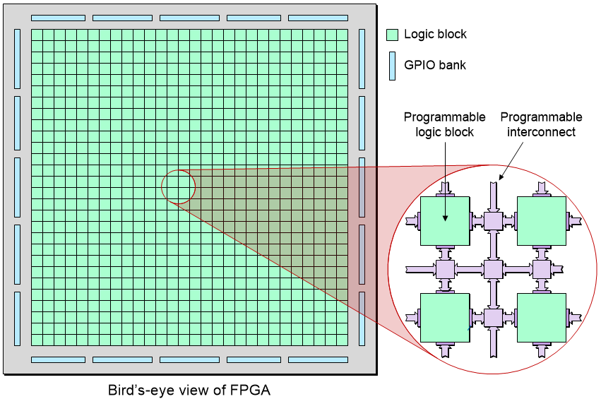
The core advantage of FPGAs lies in their unparalleled flexibility. Unlike ASICs (Application-Specific Integrated Circuits), which are designed and manufactured once for a specific task, FPGAs can be infinitely reprogrammed and reconfigured after deployment to adapt to changing requirements, support new protocols, and even fix potential hardware bugs. This significantly reduces development costs and risks, and shortens time to market. Imagine being able to improve performance or add new features through software updates even after a hardware product leaves the factory—a feat unimaginable in traditional hardware. Furthermore, FPGAs excel at parallel processing. They integrate a large number of configurable logic blocks, memory cells, and routing resources, which can be efficiently organized to execute multiple operations simultaneously at the hardware level. This inherent parallelism makes FPGAs excel in applications that require high throughput, ultra-low latency, and real-time responsiveness. These include real-time data processing, complex image recognition algorithms, acceleration tasks in high-performance computing clusters, and ultra-low latency systems in financial trading, all of which fully leverage the enormous advantages of parallel processing.
Similarities and Differences between FPGAs and CPUs/GPUs
To better understand the unique value of FPGAs, it's necessary to compare them in depth with common processors currently on the market. The CPU (central processing unit), the "brain" of a computer, excels at serial processing—executing operations sequentially according to a stream of instructions. Its versatility and powerful instruction make it the preferred choice for handling complex logic and general-purpose computing tasks. GPUs (graphics processing units), on the other hand, possess a massive number of computing cores and excel at parallelizing many simple, repetitive computational tasks. They are particularly well-suited for graphics rendering, scientific computing, and, in recent years, deep learning model training. FPGAs, however, sit somewhere in between these two, offering a new paradigm for hardware acceleration. Unlike CPUs and GPUs, FPGAs allow users to directly define data flow and control logic at the hardware level, achieving higher levels of parallelism than CPUs. Furthermore, they can accelerate certain algorithms with lower latency and higher energy efficiency than GPUs. In short, when extreme customization, ultra-low latency, and specialized, highly parallel computing are required, FPGAs are often the best choice. They can "burn" software algorithms into hardware circuits, achieving a leap in performance.
FPGA Applications
FPGAs' unique characteristics and powerful capabilities have led to their widespread application in a wide range of fields. In data centers, FPGAs are widely used to accelerate AI inference, implement network function virtualization (NFV), and perform high-performance data compression and encryption tasks, significantly improving data center processing efficiency and responsiveness. In the communications sector, they are core components for building high-performance base stations, radio units, and next-generation network equipment, supporting the deployment of advanced communication technologies such as 5G. In the automotive industry, FPGAs play a key role in advanced driver assistance systems (ADAS) and autonomous driving, processing massive amounts of data from sensors such as cameras, radar, and lidar in real time and making rapid decisions. Furthermore, medical imaging equipment requires FPGAs for high-precision data acquisition and image reconstruction; in industrial automation, FPGAs are used to implement complex real-time control systems and machine vision; and in the aerospace sector, the high reliability and reconfigurability of FPGAs are used to design critical airborne systems and satellite communications equipment. These are just the tip of the iceberg; the potential of FPGAs is continuously being explored, permeating every aspect of our lives.
With the rapid development of artificial intelligence, machine learning, and edge computing, the demand for high-performance, low-power, and highly customizable computing capabilities is growing. FPGAs hold enormous potential for future development. Their programmability and exceptional performance make them an ideal choice for meeting tomorrow's complex computing challenges. We anticipate the emergence of more powerful and highly integrated FPGA chips, accompanied by easier-to-use development tools and a more comprehensive ecosystem. This will significantly lower the barrier to entry for FPGA development, enabling their adoption and application by a wider range of developers.
One-Stop HDI PCB Manufacturer and Its PCB Via Filing Capabilities
If you're looking for turnkey HDI electronics manufacturing services (EMS) from hardware development to PCBA fabrication and box-build assembly, you can work with the one-stop HDI PCBA manufacturer PCBONLINE.
Founded in 1999, PCBONLINE has R&D capabilities for HDI projects and EMS manufacturing capabilities, including via filling for stacked vias. It provides 4-to-64-layer HDI PCB fabrication, assembly, and PCBA box-build assembly. You can order various HDI PCBs from PCBONLINE, such as FR4, polyimide (flexible PCB), polyimide + FR4 (rigid-flex PCB), and PTFE/Rogers (high-frequency PCB).

3000m² of production capacity per day for HDI PCBs with builds of 1+N+1, 2+N+2, 3+N+3,4+N+4, and arbitrary interconnection in any layers.
PCBONLINE has hardware and software R&D capabilities for IoT applications requiring HDI design, including PCBA and enclosures.
We can manufacture complex PCBs with stacker vias, via-in-pad, microvias, inlay boards, heavy copper designs, and hybrid and fine structure lay-ups.
Besides HDI PCB fabrication, we have powerful capabilities in fine-pitch assembly for HDI PCB assembly.
We have rich R&D and manufacturing experience for HDI applications such as FPGA boards.
High-quality HDI PCB and PCBA manufacturing certified with ISO 9001:2015, IATF 16949, RoHS, REACH, UL, and IPC-A-610 Class 2/3.
Here'e the PCB via filing capabilities at PCBONLINEL:
- Micriavia filling with copper: laser via size 0.1-0.125mm, priority 0.1mm
- Finished hole size for via-in-pad filling with resin: 0.1-0.9mm (drill size 0.15-1.0mm), 0.3-0.55mm normal (drill size 0.4-0.65mm)
- Max aspect ratio for via-in-pad filling with resin PCB - 12: 1
- Min resin plugged PCB thickness: 0.2mm
- Max via-filling ith resin PCB thickness: 3.2mm
- Making different hole sizes with via filling in one board: Yes
- Via filling with copper/silver: Yes
If you need HDI PCBAs or any other PCBAs requiring via filling, please send your email to PCBONLINE at info@pcbonline.com. We will provide one-on-one engineering support to you.
Conclusion
Via filling is used for creating stacked vias in HDI PCB fabrication, BGA/CSP/QFN IC packaging, and filling PCB via-in-pad with resin during multilayer PCB fabrication. If you need one-stop electronics manufacturing for your HDI PCBA project, contact the one-stop advanced PCB manufacturer PCBONLINE for high-quality PCBA and box-build solutions tailored to your project's needs.
PCB fabrication at PCBONLINE.pdf


