
When a server motherboard is scrapped in batches due to ENIG black disk defects, when millions of consumer electronic products are urgently recalled due to HASL bridging - the fatal trap of surface treatment is eating up profits. Data shows that choosing the wrong process can cause the rework cost to soar 50 times, and the misuse of HASL in high-frequency circuits causes a surge in signal loss by 83%. This article will use 12 sets of key data to tear open the veil of truth about ENIG and HASL, and take you through the technical minefields of five life and death dimensions: from the fatal threshold of black disk phosphorus content (>8%), to the thickness difference of HASL crescent effect (25μm), from the life and death line of $0.5 and $8 per square meter cost, to the life strangulation of 12,000 and 8,500 vibration tests... This is not a processed choice, but a matter of product survival.
In this article:
Part 1. What are ENIG and HASL? Part 2. Difference between Performance and Cost Part 3. Application Differences in Different ScenariosWhat are ENIG and HASL?
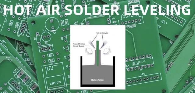
HASL (hot air solder leveling)
The traditional HASL process forms a protective coating by immersing the PCB in molten solder (tin-lead or lead-free alloy) and then using a hot air knife to blow away the excess tin layer. Its core value lies in low cost and high soldering strength. It was the mainstream technology for surface treatment in the 1980s47. The emergence of lead-free HASL further solves environmental compliance issues (such as RoHS requirements)14.
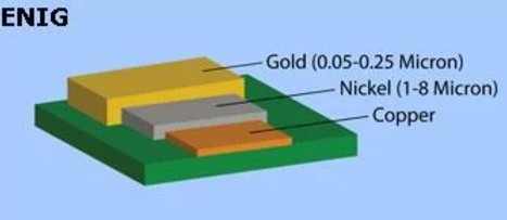
ENIG (electroless nickel immersion gold)
ENIG uses a chemical deposition method to first plate a layer of nickel (3-6μm) on the copper surface and then plate an extremely thin layer of gold (0.05-0.125μm). Nickel acts as a barrier layer to prevent copper diffusion, while gold ensures solderability and oxidation resistance. Its greatest advantage lies in surface flatness and stability, which is especially suitable for high-density packaging scenarios15.
Difference between Performance and Cost
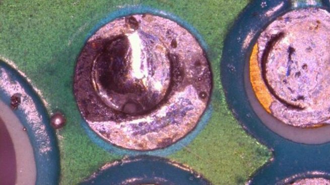
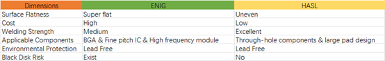
ENIG, with its ultra-flat surface (<0.05μm), crushes the "crescent effect" of HASL (thickness difference of up to 25μm), becoming the only choice for 01005 components and 0.3mm BGA packages. Its gold layer roughness (Ra 0.1-0.2μm) ensures the integrity of 5GHz+ high-frequency signals - but there is a potential risk of "black disk" caused by uncontrolled phosphorus content (solder joint strength drops by 40%). On the other hand, HASL's tin layer oxidation compresses the welding window to 48 hours, and the IMC layer thickening rate after repeated thermal cycles is 2.3 times that of ENIG, but the solder joint's vibration resistance (first failure cycle 12,000 times) is significantly better than ENIG (8,500 times), and it is more resilient in mechanical stress scenarios.
HASL dominates the consumer electronics market with a cost of $0.5-1.2/㎡ (1/6 of ENIG) and $80,000 in equipment investment (ENIG requires $250,000), but its 3.5% rework rate brings hidden costs. Although ENIG has a unit price of $5-8/㎡ and wastewater treatment accounts for 18% of the cost, the 1.2% rework rate and 12-month storage period are suitable for high value-added products. In terms of environmental protection, the high temperature of 265℃ of the lead-free version of HASL causes the expansion rate of the FR4 substrate to rise to 4.2%, and the cyanide wastewater of ENIG needs professional treatment - both require additional costs for green manufacturing.
Application Differences in Different Scenarios
When BGA packaging is absent, signal rate is less than 1GHz and budget is less than $5/㎡, HASL is a rational choice. The car entertainment system solves the bridge defect through the tin-stealing pad design, and the home appliance control board maintains the profit line with its low-cost repair of $0.3/point. The case of a car radio with an annual output of 500,000 pieces proves that the HASL solution can save $215,000/year, but it has to bear the cost of a 15μm drop in the alignment accuracy of the multi-layer board due to thermal deformation.
ENIG is the only solution for 5G base station 28GHz signals (insertion loss is 0.8dB/m lower than HASL), medical equipment -40℃~+85℃ thousand times thermal shock test, or gold wire bonding (>8gf strength). Pacemaker circuits and server motherboards would rather bear the high rework cost of $0.8/point in exchange for the stability of more than 12 months of storage period and 3 times of 260℃ reflow soldering - this is a battlefield where money is used to buy reliability.
There is no best choice. It is about the balance between the smooth surface of the circuit board and the solid solder joints, the precision angle and the cost angle. The choice between ENIG and HASL depends on the engineer's balance between reliability and cost.
One-Stop HDI PCB Manufacturer and Its PCB Via Filing Capabilities
If you're looking for turnkey HDI electronics manufacturing services (EMS) from hardware development to PCBA fabrication and box-build assembly, you can work with the one-stop HDI PCBA manufacturer PCBONLINE.
Founded in 1999, PCBONLINE has R&D capabilities for HDI projects and EMS manufacturing capabilities, including via filling for stacked vias. It provides 4-to-64-layer HDI PCB fabrication, assembly, and PCBA box-build assembly. You can order various HDI PCBs from PCBONLINE, such as FR4, polyimide (flexible PCB), polyimide + FR4 (rigid-flex PCB), and PTFE/Rogers (high-frequency PCB).

3000m² of production capacity per day for HDI PCBs with builds of 1+N+1, 2+N+2, 3+N+3,4+N+4, and arbitrary interconnection in any layers.
PCBONLINE has hardware and software R&D capabilities for IoT applications requiring HDI design, including PCBA and enclosures.
We can manufacture complex PCBs with stacker vias, via-in-pad, microvias, inlay boards, heavy copper designs, and hybrid and fine structure lay-ups.
Besides HDI PCB fabrication, we have powerful capabilities in fine-pitch assembly for HDI PCB assembly.
We have rich R&D and manufacturing experience for HDI applications such as FPGA boards.
High-quality HDI PCB and PCBA manufacturing certified with ISO 9001:2015, IATF 16949, RoHS, REACH, UL, and IPC-A-610 Class 2/3.
Here'e the PCB via filing capabilities at PCBONLINEL:
- Micriavia filling with copper: laser via size 0.1-0.125mm, priority 0.1mm
- Finished hole size for via-in-pad filling with resin: 0.1-0.9mm (drill size 0.15-1.0mm), 0.3-0.55mm normal (drill size 0.4-0.65mm)
- Max aspect ratio for via-in-pad filling with resin PCB - 12: 1
- Min resin plugged PCB thickness: 0.2mm
- Max via-filling ith resin PCB thickness: 3.2mm
- Making different hole sizes with via filling in one board: Yes
- Via filling with copper/silver: Yes
If you need HDI PCBAs or any other PCBAs requiring via filling, please send your email to PCBONLINE at info@pcbonline.com. We will provide one-on-one engineering support to you.
Conclusion
Via filling is used for creating stacked vias in HDI PCB fabrication, BGA/CSP/QFN IC packaging, and filling PCB via-in-pad with resin during multilayer PCB fabrication. If you need one-stop electronics manufacturing for your HDI PCBA project, contact the one-stop advanced PCB manufacturer PCBONLINE for high-quality PCBA and box-build solutions tailored to your project's needs.
PCB fabrication at PCBONLINE.pdf


