
In modern society, electricity powers every aspect of our lives. However, not all electricity exists in the form we are most familiar with. For example, power from solar panels and batteries is direct current (DC), while the vast majority of appliances in our homes use alternating current (AC). This difference in these two current forms necessitates the critical need for DC-to-AC conversion. This article will delve into the core principles of this conversion process, key devices, and different types of options, helping you understand how to efficiently and safely convert energy from the sun or stored energy from batteries into the electricity we use every day.
In this article:
Part 1. Why Do We Need to Convert DC to AC? Part 2. The Inverter: The Key Device for Conversion Part 3. How an Inverter Works: From Square Wave to Sine Wave Part 4. Choosing the Right Inverter: Consider Your NeedsWhy Do We Need to Convert DC to AC?
In our daily lives, nearly all household appliances, such as televisions, refrigerators, and lights, rely on alternating current (AC) to operate. However, many renewable energy sources, such as solar panels and batteries, generate direct current (DC). Therefore, to effectively utilize this energy, we need a method to convert DC to AC. This process is not only crucial for powering homes but is also widely used in electric vehicles, UPS (uninterruptible power supply) systems, and various industrial equipment. Understanding this conversion process is crucial to the operation of modern power systems, ensuring that we can seamlessly integrate power from different sources into existing power grids.
The Inverter: The Key Device for Conversion
The key device for converting direct current (DC) to alternating current (AC) is the inverter. An inverter is an electronic device that receives DC input from batteries or solar panels and, through a complex series of electronic switching operations, converts it to the AC output needed by our homes and businesses. The working principle of an inverter can be simplified by rapidly opening and closing switches to simulate the waveform of an AC sine wave. This process requires sophisticated control circuitry to ensure stable output voltage and frequency, matching the voltage and frequency of the standard power grid.
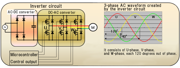
How an Inverter Works: From Square Wave to Sine Wave
An inverter typically operates in several stages. First, it receives a constant DC input voltage. Then, using a set of semiconductor switches (such as MOSFETs or IGBTs), the inverter rapidly switches the direction of the current at a certain frequency, generating a rough AC signal known as a square wave. While this square wave is AC, its waveform quality is poor and unsuitable for driving most sensitive electronic devices. To achieve high-quality AC, the inverter uses one or more filters (typically a combination of capacitors and inductors) to smooth the square wave, gradually bringing it closer to a perfect sine wave. Finally, a transformer steps the voltage up or down, and a feedback control system fine-tunes the output waveform to ensure the AC is stable and pure enough to safely power any household appliance.
Choosing the Right Inverter: Consider Your Needs
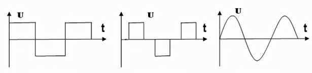
There are many different types of inverters available on the market, and choosing the right one depends on your specific application. There are three main types of inverters: square wave inverters, modified sine wave inverters, and pure sine wave inverters. Square wave inverters are the cheapest, but their output waveform is poor quality, making them suitable only for driving simple, non-inductive loads such as incandescent lamps. Modified sine wave inverters are the most common and affordable type, capable of driving most appliances, but may produce harmonic interference with some delicate electronic devices and motors. Pure sine wave inverters, on the other hand, produce a waveform identical to the mains power. They are the most efficient and safest option, suitable for all types of appliances, especially those requiring high-quality power, such as computers, medical equipment, and induction motors. Although pure sine wave inverters are the most expensive, they provide the most reliable power.
In short, converting direct current (DC) to alternating current (AC) is an essential technology. Inverters are at its core, transforming energy from batteries or solar panels into electricity for use in homes and industries. From simple square waves to high-quality pure sine waves, different types of inverters meet various application requirements. With the proliferation of renewable energy and the rise of smart grids, inverter technology is becoming increasingly efficient and intelligent. Understanding this conversion process not only helps us better utilize clean energy but also provides a solid foundation for future energy management and power systems, ensuring our world operates sustainably and efficiently.
One-Stop HDI PCB Manufacturer and Its PCB Via Filing Capabilities
If you're looking for turnkey HDI electronics manufacturing services (EMS) from hardware development to PCBA fabrication and box-build assembly, you can work with the one-stop HDI PCBA manufacturer PCBONLINE.
Founded in 1999, PCBONLINE has R&D capabilities for HDI projects and EMS manufacturing capabilities, including via filling for stacked vias. It provides 4-to-64-layer HDI PCB fabrication, assembly, and PCBA box-build assembly. You can order various HDI PCBs from PCBONLINE, such as FR4, polyimide (flexible PCB), polyimide + FR4 (rigid-flex PCB), and PTFE/Rogers (high-frequency PCB).

3000m² of production capacity per day for HDI PCBs with builds of 1+N+1, 2+N+2, 3+N+3,4+N+4, and arbitrary interconnection in any layers.
PCBONLINE has hardware and software R&D capabilities for IoT applications requiring HDI design, including PCBA and enclosures.
We can manufacture complex PCBs with stacker vias, via-in-pad, microvias, inlay boards, heavy copper designs, and hybrid and fine structure lay-ups.
Besides HDI PCB fabrication, we have powerful capabilities in fine-pitch assembly for HDI PCB assembly.
We have rich R&D and manufacturing experience for HDI applications such as FPGA boards.
High-quality HDI PCB and PCBA manufacturing certified with ISO 9001:2015, IATF 16949, RoHS, REACH, UL, and IPC-A-610 Class 2/3.
Here'e the PCB via filing capabilities at PCBONLINEL:
- Micriavia filling with copper: laser via size 0.1-0.125mm, priority 0.1mm
- Finished hole size for via-in-pad filling with resin: 0.1-0.9mm (drill size 0.15-1.0mm), 0.3-0.55mm normal (drill size 0.4-0.65mm)
- Max aspect ratio for via-in-pad filling with resin PCB - 12: 1
- Min resin plugged PCB thickness: 0.2mm
- Max via-filling ith resin PCB thickness: 3.2mm
- Making different hole sizes with via filling in one board: Yes
- Via filling with copper/silver: Yes
If you need HDI PCBAs or any other PCBAs requiring via filling, please send your email to PCBONLINE at info@pcbonline.com. We will provide one-on-one engineering support to you.
Conclusion
Via filling is used for creating stacked vias in HDI PCB fabrication, BGA/CSP/QFN IC packaging, and filling PCB via-in-pad with resin during multilayer PCB fabrication. If you need one-stop electronics manufacturing for your HDI PCBA project, contact the one-stop advanced PCB manufacturer PCBONLINE for high-quality PCBA and box-build solutions tailored to your project's needs.
PCB fabrication at PCBONLINE.pdf


