
Many people are familiar with COB but are unfamiliar with it. This blog will discover how COB’s bare-die integration enables smaller, cheaper, and more reliable devices across industries.
In this article:
Part 1. What Is Chip on Board (COB)? Defining the Core Technology Part 2. COB vs. Alternative Packaging: Where Does It Stand? Part 3. Top 5 Advantages Driving COB Adoption Part 4. Dominant Applications Across IndustriesWhat Is Chip on Board (COB)? Defining the Core Technology
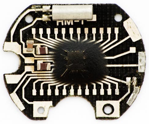
Chip on Board (COB) is an advanced semiconductor packaging method where unpackaged silicon dies are mounted directly onto a printed circuit board (PCB), electrically connected via wire bonding, and protected by epoxy encapsulation. Unlike traditional packaging, COB eliminates plastic/metal casings, slashing costs while boosting thermal and spatial efficiency.
Key characteristics:
- Bare-Die Integration: Chips attach face-up to PCBs.
- Wire Bonding: Gold/aluminum wires link die pads to substrate traces.
COB vs. Alternative Packaging: Where Does It Stand?
COB vs. SMT (Surface Mount Technology)
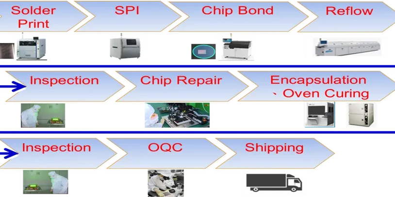
COB manufacturing relies on four precision-driven stages. First, substrate preparation ensures the PCB surface is contaminant-free through ionized air cleaning—critical for strong chip adhesion. Next, die attachment secures the bare silicon chip using conductive silver paste or non-conductive epoxy. The third phase, wire bonding, creates electrical pathways: Gold or aluminum wires connect the chip’s bond pads to the PCB using either ball bonding (for high-speed ICs) or ultrasonic wedge bonding (for fine-pitch applications like sensors). Finally, a protective epoxy encapsulant (often black or thermally conductive resin) is dispensed over the assembly, shielding it from moisture, dust, and mechanical stress before curing under UV light or heat. This streamlined flow contrasts sharply with multi-step conventional packaging, cutting lead times by 30–50%.
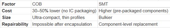
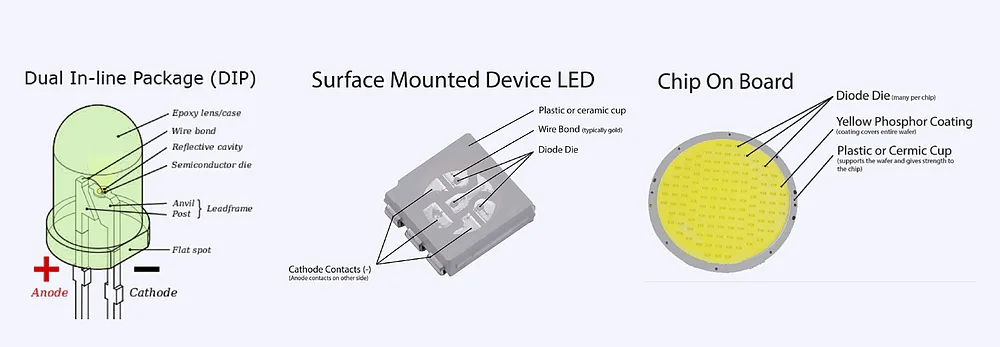
When compared to Surface Mount Technology (SMT), COB’s elimination of individual packages enables thinner profiles (0.8mm vs. 2mm) and lower parasitic capacitance—crucial for 5G RF modules. However, SMT allows easier component replacement during repairs. Against Flip Chip techniques, COB’s wire-bonded interfaces simplify manufacturing but limit I/O density. Flip Chip’s solder bumps support 10,000+ connections per chip (vs. COB’s typical 500), making it preferable for GPU/CPU dies, albeit at 3× the cost. Chip-on-Glass (COG), a COB variant, bonds ICs directly to LCD panels using anisotropic conductive film. While COG enables razor-thin displays in smartwatches, its glass substrates are more fragile than COB’s fiberglass PCBs for industrial gear.
COB vs. Flip Chip
- Flip Chip: Dies face down, solder bumps connect to substrate. Superior electrical performance but requires costly redistribution layers (RDLs).
- COB: Simpler wire bonding, lower thermal resistance, ideal for cost-sensitive applications.
Top 5 Advantages Driving COB Adoption
1.Space Savings
Eliminates bulky IC packages—critical for wearables, smartphones, and IoT devices.
2.Thermal Management
Direct PCB contact + thermal epoxies reduce junction temperatures by 15–25°C vs. SMT.
3.Cost Efficiency
Up to 60% lower production costs for high-volume runs (e.g., LED lighting).
4.Enhanced Reliability
Resins block moisture, dust, and vibrations—extending product lifespans in harsh environments.
5.Optical Performance
COB LEDs deliver uniform, glare-free illumination—ideal for automotive headlights and stadium lighting.
Limitations and Design Challenges
- Irreversible Repairs: Failed chips can’t be replaced post-encapsulation.
- Signal Integrity Risks:
- Long wire bonds increase inductance, disrupting high-frequency signals.
- CTE (thermal expansion) mismatches may crack bonds during thermal cycling.
- Process Sensitivity: Requires Class 100–1000 cleanrooms to prevent particulate contamination.
Dominant Applications Across Industries
LED Lighting leverages COB most aggressively. High-lumen COB arrays (e.g., 100W LED panels) deliver uniform, glare-free illumination for stadium lights and surgical lamps—doubling the lifespan of SMT-based alternatives. Consumer Electronics integrates COB in miniature cameras, where 10+ LEDs fit into smartphone flash modules, and voice-assistant microphones requiring noise-immune signal paths. Automotive Systems rely on COB for ECU control boards and LiDAR sensors, where vibration resistance ensures reliability at 150°C engine temperatures. Emerging frontiers include biomedical implants (pacemakers with epoxy-sealed ASICs) and agricultural IoT—soil sensors with humidity-proof COB circuits surviving harsh field environments for years.
In all, Chip on Board technology exemplifies how elegance in engineering drives progress. By stripping away non-essential packaging, COB achieves unprecedented power density, thermal performance, and cost efficiency—cornerstones of tomorrow’s electronics. Though challenges around repairability and process control persist, relentless innovation in bonding techniques and encapsulation materials continues to expand its horizons. From smart cities to personalized healthcare, COB’s invisible hand will keep powering the devices reshaping our world.
One-Stop HDI PCB Manufacturer and Its PCB Via Filing Capabilities
If you're looking for turnkey HDI electronics manufacturing services (EMS) from hardware development to PCBA fabrication and box-build assembly, you can work with the one-stop HDI PCBA manufacturer PCBONLINE.
Founded in 1999, PCBONLINE has R&D capabilities for HDI projects and EMS manufacturing capabilities, including via filling for stacked vias. It provides 4-to-64-layer HDI PCB fabrication, assembly, and PCBA box-build assembly. You can order various HDI PCBs from PCBONLINE, such as FR4, polyimide (flexible PCB), polyimide + FR4 (rigid-flex PCB), and PTFE/Rogers (high-frequency PCB).

3000m² of production capacity per day for HDI PCBs with builds of 1+N+1, 2+N+2, 3+N+3,4+N+4, and arbitrary interconnection in any layers.
PCBONLINE has hardware and software R&D capabilities for IoT applications requiring HDI design, including PCBA and enclosures.
We can manufacture complex PCBs with stacker vias, via-in-pad, microvias, inlay boards, heavy copper designs, and hybrid and fine structure lay-ups.
Besides HDI PCB fabrication, we have powerful capabilities in fine-pitch assembly for HDI PCB assembly.
We have rich R&D and manufacturing experience for HDI applications such as FPGA boards.
High-quality HDI PCB and PCBA manufacturing certified with ISO 9001:2015, IATF 16949, RoHS, REACH, UL, and IPC-A-610 Class 2/3.
Here'e the PCB via filing capabilities at PCBONLINEL:
- Micriavia filling with copper: laser via size 0.1-0.125mm, priority 0.1mm
- Finished hole size for via-in-pad filling with resin: 0.1-0.9mm (drill size 0.15-1.0mm), 0.3-0.55mm normal (drill size 0.4-0.65mm)
- Max aspect ratio for via-in-pad filling with resin PCB - 12: 1
- Min resin plugged PCB thickness: 0.2mm
- Max via-filling ith resin PCB thickness: 3.2mm
- Making different hole sizes with via filling in one board: Yes
- Via filling with copper/silver: Yes
If you need HDI PCBAs or any other PCBAs requiring via filling, please send your email to PCBONLINE at info@pcbonline.com. We will provide one-on-one engineering support to you.
Conclusion
Via filling is used for creating stacked vias in HDI PCB fabrication, BGA/CSP/QFN IC packaging, and filling PCB via-in-pad with resin during multilayer PCB fabrication. If you need one-stop electronics manufacturing for your HDI PCBA project, contact the one-stop advanced PCB manufacturer PCBONLINE for high-quality PCBA and box-build solutions tailored to your project's needs.
PCB fabrication at PCBONLINE.pdf


