
In today's era of rapid evolution toward electrification, intelligence, and connectivity in the automotive industry, vehicles are no longer merely collections of mechanical components but highly integrated “supercomputers on wheels.” In this process, printed circuit boards (PCBs) serve as the physical foundation and nerve center for all electronic systems. Their reliability, performance, and quality directly determine the vehicle's safety, functionality, and durability. Consequently, a rigorous, comprehensive, and continuously evolving professional standard system—the “Automotive PCB Standards”—has become the lifeline safeguarding the quality of modern automotive electronics. These standards are not only the “code” manufacturers must adhere to, but also the framework driving PCB design, material selection, manufacturing processes, and testing verification toward excellence. This article will delve into the core standard system for automotive PCBs and provide a detailed interpretation of the critical precision manufacturing processes behind them, revealing the technical depth of this high-reliability electronics domain to readers.
In this article:
Part 1. Core Concepts and Global Standards for PCB Panels Part 2. Multi-dimensional Considerations for Panel Size Selection Part 3. Panelization Design Practices and Industry TrendsCore Standard System for Automotive PCBs
The automotive electronics operating environment is extremely harsh, requiring components to withstand extreme temperature cycles ranging from -40°C to over 150°C, high-intensity vibration, humidity, chemical corrosion, and complex electromagnetic environments. Consequently, generic PCB standards designed for consumer electronics are wholly inadequate here. Automotive PCB standards form a multi-layered, cross-disciplinary ecosystem primarily built around reliability, quality, and consistency.
Their core principles typically originate from international organizations such as the International Electrotechnical Commission (IEC) and the Institute of Electrical and Electronics Engineers (IEEE). However, the most binding and influential standards are proprietary specifications developed collaboratively by global automakers and their supply chains. Among these, IPC (International Electronics Manufacturing Alliance) standards form the foundation for manufacturing and acceptance, particularly IPC-6012 “Identification and Performance Specifications for Rigid Printed Boards” and its automotive addendum IPC-6012DA. This document imposes requirements far exceeding standard industrial grades—specifically “Class 3” or higher—for automotive PCBs regarding dimensions, plating, via copper thickness, dielectric layers, and surface finishes. For instance, critical via copper thickness for high-reliability applications must reach at least 25 microns to prevent plating cracking under thermal stress.
However, the true “crown jewel” lies in standards led by automotive manufacturers. Standards from the German Association of the Automotive Industry (VDA), particularly the DIN EN 60068-2 series of environmental testing standards developed in collaboration with the German Institute for Standardization (DIN), serve as the benchmark for the German supply chain. Globally influential is undoubtedly the IATF 16949:2016 quality management system standard promoted by the Automotive Industry Action Group (AIAG). While not specifically tailored for PCBs, it mandates that all automotive component suppliers—including PCB manufacturers—operate their quality systems based on this framework. It enforces core tools such as Advanced Product Quality Planning (APQP), Production Part Approval Process (PPAP), Failure Mode and Effects Analysis (FMEA), and Statistical Process Control (SPC). This means PCBs are subject to rigorous quality management throughout their entire lifecycle—from design reviews and material certification to process monitoring and final delivery.

Additionally, major original equipment manufacturers (OEMs) maintain their own detailed factory standards, such as Ford's WSS-M99P series, General Motors' GMW 3172, and Daimler's DIN 72570. These standards build upon universal international/industry standards by imposing more specific, customized limit requirements for particular performance characteristics—such as high-temperature cycle endurance, vibration spectrum resistance, and CAF resistance to conductive anode wire. For example, in PCBs for high-power modules in electric vehicles, thermal conductivity, dielectric strength, and resistance to electromigration become focal points of the standards. Collectively, these standards form an impenetrable quality assurance network, ensuring that even a tiny PCB within a mass-produced vehicle operates reliably throughout its entire service life.
Precision Material Engineering for High-Reliability Automotive PCBs
The selection of materials directly determines the mechanical, electrical, and thermal performance boundaries of PCBs in extreme environments. The rigor and specificity of this selection process are hallmarks distinguishing automotive applications from other fields.
For substrate materials, high-performance FR-4 epoxy glass cloth laminates are most commonly used, but their specific formulations—such as glass transition temperature (Tg), decomposition temperature (TD), and coefficient of thermal expansion (CTE)—are critical. For PCBs near the engine compartment or within the powertrain, standards typically mandate high-Tg (generally ≥170°C), medium-Tg, or even ultra-high-Tg materials (e.g., FR-4 with Tg ≥180°C or halogen-free alternatives) to resist material softening, delamination, or electrical degradation caused by prolonged exposure to high temperatures. For radar and V2X antenna boards involving high-frequency applications, low-loss (low Dk/Df) RF materials like polytetrafluoroethylene (PTFE) or hydrocarbon ceramics are essential to ensure signal integrity. For power module PCBs in IGBT drivers and DC-DC converters, metal substrates (e.g., aluminum substrate IMS) or direct bonded copper (DBC) ceramic substrates are widely adopted due to their superior thermal conductivity. Standards strictly specify the thermal conductivity, breakdown voltage, and bond strength of the insulating layer.

Copper foil serves as the carrier for conductive pathways. Automotive PCBs commonly utilize highly ductile electrolytic copper foil (HDI) or reverse-tinned foil (RTF), whose surface roughness is optimized to ensure strong bonding with the substrate while minimizing “skin effect” losses during high-frequency signal transmission. Standards clearly define copper foil purity, tensile strength, and elongation to withstand thermal cycling stresses.
Surface treatment processes protect copper pads and ensure solderability. Mainstream eco-friendly processes like Electrolytic Nickel Palladium Gold (ENEPIG) and Electrolytic Nickel Immersion Gold (ENIG) are widely used in automotive controllers due to their flat surfaces, excellent solderability, and long shelf life. For high-current contacts or connector areas, hard gold plating or selective silver plating may be employed. Each process adheres to stringent standards governing thickness, composition, and porosity. For instance, ENIG typically requires a nickel layer thickness of 3-5 microns and a gold layer of 0.05-0.1 microns to prevent soldering defects like “black nickel” or “gold embrittlement.”


Additionally, solder mask inks must exhibit high thermal resistance, strong adhesion, excellent insulation resistance, and chemical corrosion resistance (e.g., moisture and fuel resistance). The material certification process is exceptionally lengthy, requiring a series of compatibility, reliability, and accelerated life tests against relevant standards (such as UL94 V-0 flame retardancy rating) before inclusion in an OEM's Qualified Materials List (QML). This constitutes a standards-driven, deep material engineering endeavor.
Key Manufacturing Processes
Within a rigorous standards framework and on the foundation of precision materials, the manufacturing process is the decisive step in transforming design into qualified products. The production of automotive PCBs involves a series of high-tech, high-precision control processes, with each step required to meet or exceed standard specifications.
Pattern formation and inner layer fabrication mark the starting point. Replacing traditional film exposure with Laser Direct Imaging (LDI) technology enables finer traces (line width/spacing as small as 75μm/75μm is common for automotive electronics) and enhanced alignment accuracy, meeting high-density interconnect requirements. Following inner layer etching, automated optical inspection (AOI) is conducted at 100% coverage to detect any open circuits, short circuits, or notch defects. Standards enforce an extremely strict zero-tolerance policy for acceptable defect sizes.
Laminating multilayer boards is central to building reliability. Stack-up alignment precision, prepreg (PP sheet) flow, and curing cycles are precisely controlled to ensure void-free layers, complete resin fill, and uniform dielectric thickness. Post-lamination non-destructive testing via ultrasonic scanning microscopy (C-SAM) is performed to identify internal defects like delamination, cracks, or voids against standards.
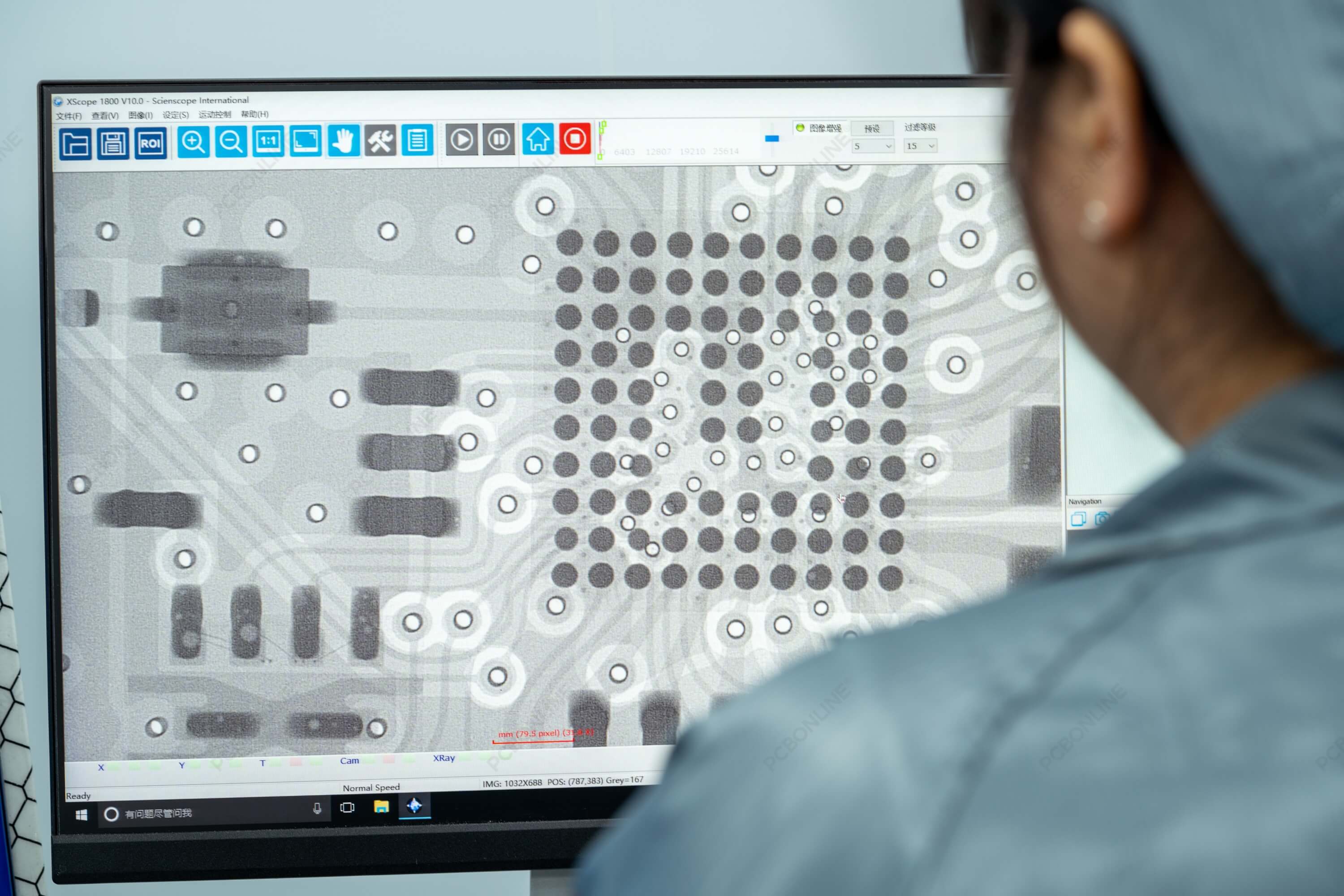
Drilling and via plating establish the physical pathways for electrical interconnections, presenting significant process challenges. For high-reliability automotive boards, the wall quality of through-holes, blind vias, and buried vias is critical. High-precision CNC drilling machines and premium drill bits, combined with optimized drilling parameters, achieve smooth hole walls. Subsequent deburring and electroless copper plating processes must be thorough to ensure excellent adhesion between the subsequent electroplated copper and the hole walls. The full-board plating and pattern plating processes strictly adhere to standard requirements for via copper thickness (e.g., minimum 25μm copper thickness at the center of through-holes). Real-time monitoring of plating solution composition, temperature, and current density, combined with techniques like pulse plating, ensures uniform and dense via copper coverage. free from “dogbone” defects or voids, enabling passage through subsequent rigorous thermal stress tests (e.g., 288°C solder float test).
Surface treatment and final shaping are equally critical. After solder mask printing and curing, the surface treatment process selected according to standards (e.g., ENEPIG) is precisely applied. The thickness of each layer is verified through random or full inspection using X-ray fluorescence (XRF) measurement instruments, with data integrated into SPC system monitoring. Final contour milling employs high-hardness carbide tools with optimized parameters to ensure smooth edges, burr-free surfaces, and no delamination, with dimensions strictly meeting design tolerances. Electrical testing (flying probe or test fixture) verifies 100% coverage of all network electrical connectivity and isolation.
Traceability is an ironclad requirement throughout automotive-grade manufacturing. From material batch numbers and serial numbers on each board to process parameters for every major operation, all data must be fully documented and linked, enabling bidirectional traceability from the final product back to the original materials. Additionally, environmental controls (cleanliness, temperature/humidity), equipment preventive maintenance, and operator certification form integral parts of the process control system. Together, these ensure every automotive PCB produced exhibits high consistency and inherent reliability.

Testing and Certification
Reliability testing is paramount. Thermal Cycle Testing (TCT) and Thermal Shock Testing (TST) subject PCBs to rapid transitions between extreme temperatures (e.g., 500-1000 cycles from -55°C to +125°C) to evaluate their resistance to fatigue failure caused by material CTE mismatch (e.g., solder joint cracking, via copper fracture). Thermal and Humidity Bias Testing (THB or HAST) applies voltage in high-temperature, high-humidity conditions to evaluate insulation performance and detect risks of Conductive Anodic Filament (CAF) growth—a hidden threat causing short-circuit failures in high-density interconnects. Mechanical vibration and shock testing simulates road bumps and impacts during vehicle operation, ensuring PCBs and soldered components remain mechanically sound under stress. Test conditions, cycles, and acceptance criteria are explicitly defined in relevant OEM or industry standards.
Additionally, Signal Integrity (SI) and Power Integrity (PI) testing are critical for PCBs in Advanced Driver Assistance Systems (ADAS) and high-speed in-vehicle networks (e.g., in-vehicle Ethernet). These tests verify compliance with design specifications for impedance control, insertion loss, return loss, and other parameters. Chemical resistance testing evaluates the PCB's ability to withstand corrosion from common automotive chemicals like brake fluid, engine oil, and gasoline.
Regarding certifications, beyond the aforementioned IATF 16949 system certification, PCB manufacturers may also pursue UL certification (safety) and ISO 14001 (environmental management). More critically, obtaining product approval from major OEM customers typically requires submitting a complete PPAP package. This includes comprehensive documentation such as material certificates, process flow diagrams, FMEA reports, dimensional reports, performance test data, and durability test reports.
Looking ahead, automotive PCB standards and processes will continue to evolve. With the proliferation of zonal architecture and autonomous driving, PCBs will advance toward higher density (HDI and even mSAP technology), higher frequency and speed, greater power density, and embedded components. Corresponding standards will increasingly focus on the reliability of any-layer HDI interconnections, ultra-low loss requirements for millimeter-wave radar boards, and new specifications for PCB insulation and creepage distances in 800V high-voltage platforms. Sustainability and carbon footprint requirements will also be progressively integrated into the standards framework. Simultaneously, artificial intelligence (AI) and the Industrial Internet of Things (IIoT) will play increasingly vital roles in process monitoring, defect prediction, and quality control, propelling manufacturing toward the goal of “zero defects.”
|
Standard System
|
Primary Focus Area
|
Key Requirements
|
|
IPC-6012DA
|
PCB Manufacturing & Acceptance
|
Stringent control of automotive-grade core process parameters
|
|
IATF 16949
|
Quality Management System
|
Mandates full-process quality control and traceability
|
|
AEC-Q200
|
Passive Component Reliability
|
Supports component-level environmental and mechanical testing
|
|
OEM-Specific Standards
|
Specific Performance & Reliability
|
Defines customized extreme testing criteria
|
Through this in-depth analysis of standards frameworks, materials science, manufacturing processes, and testing certifications, it becomes evident that the automotive PCB sector represents a standards-driven, technology-intensive, and rigorously demanding specialized domain.
One-Stop HDI PCB Manufacturer and Its PCB Via Filing Capabilities
If you're looking for turnkey HDI electronics manufacturing services (EMS) from hardware development to PCBA fabrication and box-build assembly, you can work with the one-stop HDI PCBA manufacturer PCBONLINE.
Founded in 1999, PCBONLINE has R&D capabilities for HDI projects and EMS manufacturing capabilities, including via filling for stacked vias. It provides 4-to-64-layer HDI PCB fabrication, assembly, and PCBA box-build assembly. You can order various HDI PCBs from PCBONLINE, such as FR4, polyimide (flexible PCB), polyimide + FR4 (rigid-flex PCB), and PTFE/Rogers (high-frequency PCB).

3000m² of production capacity per day for HDI PCBs with builds of 1+N+1, 2+N+2, 3+N+3,4+N+4, and arbitrary interconnection in any layers.
PCBONLINE has hardware and software R&D capabilities for IoT applications requiring HDI design, including PCBA and enclosures.
We can manufacture complex PCBs with stacker vias, via-in-pad, microvias, inlay boards, heavy copper designs, and hybrid and fine structure lay-ups.
Besides HDI PCB fabrication, we have powerful capabilities in fine-pitch assembly for HDI PCB assembly.
We have rich R&D and manufacturing experience for HDI applications such as FPGA boards.
High-quality HDI PCB and PCBA manufacturing certified with ISO 9001:2015, IATF 16949, RoHS, REACH, UL, and IPC-A-610 Class 2/3.
Here'e the PCB via filing capabilities at PCBONLINEL:
- Micriavia filling with copper: laser via size 0.1-0.125mm, priority 0.1mm
- Finished hole size for via-in-pad filling with resin: 0.1-0.9mm (drill size 0.15-1.0mm), 0.3-0.55mm normal (drill size 0.4-0.65mm)
- Max aspect ratio for via-in-pad filling with resin PCB - 12: 1
- Min resin plugged PCB thickness: 0.2mm
- Max via-filling ith resin PCB thickness: 3.2mm
- Making different hole sizes with via filling in one board: Yes
- Via filling with copper/silver: Yes
If you need HDI PCBAs or any other PCBAs requiring via filling, please send your email to PCBONLINE at info@pcbonline.com. We will provide one-on-one engineering support to you.
Conclusion
Via filling is used for creating stacked vias in HDI PCB fabrication, BGA/CSP/QFN IC packaging, and filling PCB via-in-pad with resin during multilayer PCB fabrication. If you need one-stop electronics manufacturing for your HDI PCBA project, contact the one-stop advanced PCB manufacturer PCBONLINE for high-quality PCBA and box-build solutions tailored to your project's needs.
PCB fabrication at PCBONLINE.pdf


