
This blog offers a comprehensive look at how a qualified automotive electronic unit evolves from a blueprint concept through manufacturing and quality inspection to become the reliable “nerve center” and “sensory system” within a vehicle. It is not merely a manufacturing process, but a concentrated manifestation of modern industrial reliability philosophy.
In this article:
Part 1. Manufacturing Process Part 2. Four Decisive Factors of Production Part 3. Looking Ahead - Market TrendsManufacturing Process
Pre-ManufacturingFirst comes design introduction and conversion. The engineering team meticulously reviews all design documents provided by the customer, much like an experienced architect scrutinizing blueprints. They not only ensure the design is theoretically flawless but also assess its feasibility from a manufacturing perspective—evaluating component placement for rationality, solder joint accessibility for inspection, and adequate exposure of test points. This process is the critical step in precisely translating “design language” into “manufacturing language.”
Next comes the rigorous foundation-building of the supply chain. Automotive electronics demand the utmost reliability from components. The manufacturing service provider activates a qualified supply chain system certified to IATF 16949, procuring every chip and resistor. Upon arrival, materials are not immediately sent to production lines. Instead, they undergo rigorous incoming material inspection to verify specifications, quality, and origin. Simultaneously, each batch is assigned a unique “identity card,” establishing a complete traceability record. This lays the most solid groundwork for investigating any potential issues that may arise in the future.

Manufacturing Stage
Surface mounting is the first step. Solder paste is precisely printed onto the circuit board through a stencil, followed by the placement machine positioning tiny components with dazzling speed and accuracy. Next, the reflow oven permanently “welds” them together through a precisely controlled temperature curve, forming robust electrical connections. Then, automatic optical inspection acts like an indefatigable referee, instantly judging the quality of thousands of solder joints with high-definition cameras.

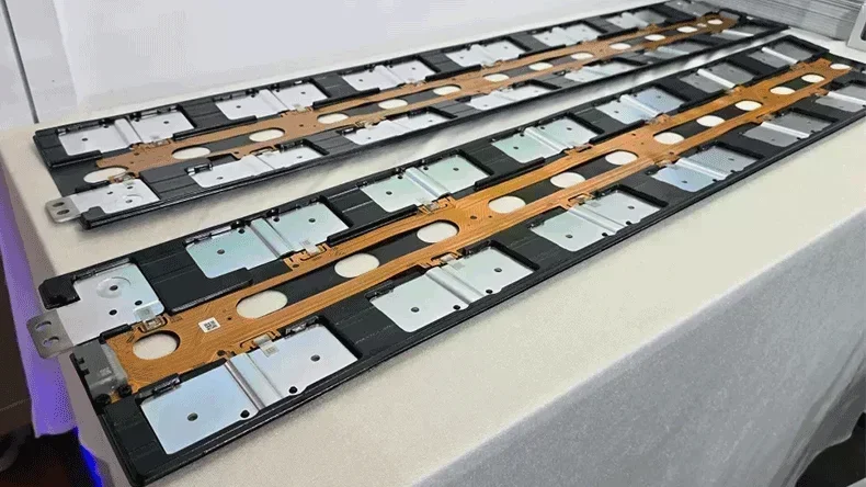
Subsequently, the product enters the system integration and soul-injection stage. The manufactured circuit board is encased in a robust housing, connected to necessary interfaces and heat sinks. Most crucially, specialized equipment “flashes” the customer's core firmware and software programs into the chip. At this point, the hardware entity is imbued with its soul, transforming from a generic circuit board into a specific automotive electronic unit—such as an ECU controlling an engine or a radar module sensing distance.
Inspection Phase
The product will be connected to a test bench simulating real automotive operating conditions to undergo comprehensive functional testing. This verifies whether it responds correctly to various commands, outputs precise signals, and meets all performance parameters. This ensures the product's “intelligence” functions properly.
Next comes the more rigorous environmental stress screening and reliability testing. Products undergo rapid temperature cycling between extreme highs and lows, continuous vibration and shock, and exposure to high-temperature, high-humidity conditions within specialized environmental chambers. This process proactively identifies and weeds out “weak links” with latent defects or short lifespans, ensuring delivered products withstand the harsh challenges throughout a vehicle's extended lifecycle.
Finally, products that pass all trials undergo final identity verification and packaging. Following a final visual inspection, they are assigned complete serial number labels and carefully packaged using shock-resistant and anti-static materials. All manufacturing processes, test data, and traceability information are fully documented. This “lifetime record” accompanies the product throughout its entire lifecycle. Only then does a qualified automotive electronic component truly complete its entire manufacturing journey, ready to be shipped to the vehicle manufacturer.
Four Decisive Factors of Production
First, the quality system. Automotive electronics manufacturing is fundamentally different from the production model of ordinary consumer electronics; it relies on a mandatory, systematic quality management system. Its core hallmark is IATF 16949 certification, which serves not only as a ticket to market access but also embodies a manufacturing philosophy centered on prevention. It deeply integrates five key tools—APQP (Advanced Product Quality Planning), FMEA (Failure Mode and Effects Analysis), PPAP (Production Part Approval Process), SPC (Statistical Process Control), and MSA (Measurement System Analysis)—into every stage of the product lifecycle, from concept design to mass production. This approach focuses on identifying and mitigating issues before they occur, systematically ensuring the reliability and consistency of the final product.
Second, Process and Manufacturing. Within this rigorous framework lie exceptionally stringent manufacturing processes and control requirements. The pursuit here is near-zero-defect first-pass yield, achieved through multi-tiered screening like high-precision SPI (Solder Inspection) and AOI (Automated Optical Inspection) to guarantee flawless solder joints. Simultaneously, full-process traceability forms the lifeline of quality accountability, requiring precise tracking of any product's production timeline, material batches, and process parameters—the cornerstone of responsibility. Furthermore, the mandatory use of AEC-Q series-certified automotive-grade components is essential, as these are specifically designed and validated to withstand the harsh environments within vehicles.

Third, validation testing. Automotive electronics must endure extreme environmental challenges throughout their lifecycle, necessitating verification standards far exceeding those of ordinary products. Rigorous, comprehensive reliability testing is indispensable, including simulated extreme temperature cycling from sub-zero to scorching conditions, prolonged high-temperature/high-humidity aging, and continuous vibration/mechanical shock simulations mimicking engine and road conditions. The purpose of these tests is to accelerate aging processes, exposing potential failures that might occur over decades of use within a short timeframe. This ensures exceptionally long-term durability and stable performance in real-world conditions.
Fourth, supply chain and management. Automotive manufacturing demands consistent, daily deliveries sustained over years, making supply chain robustness and management capabilities critical. This entails not only selecting high-quality suppliers who meet automotive standards but also establishing robust risk mitigation mechanisms—such as dual-sourcing critical materials to prevent supply disruptions. More importantly, once a product enters mass production, any changes to materials, processes, or designs must undergo stringent control. These modifications must follow formal engineering change procedures and be resubmitted for approval to prevent unforeseen risks, thereby maintaining product consistency and reliability throughout the entire production cycle.

Looking Ahead - Market Trends
Currently, the automotive electronics manufacturing services (EMS) market is experiencing a dynamic growth cycle. This momentum stems not from a single factor, but from the combined effects of the automotive industry's “new four modernizations” (electrification, intelligence, connectivity, and sharing) and profound supply chain transformations, reshaping the entire industry landscape.
The market expansion stems primarily from the increasing complexity and value of automotive electronic architectures. While electronics may account for less than 30% of the cost in traditional fuel-powered vehicles, this figure can easily exceed 50% in a pure electric smart car. This growth is driven by tangible incremental demand:
More importantly, the industry's value center is undergoing a quiet yet profound shift. It is no longer confined solely to hardware manufacturing itself, but is accelerating toward integrated “hardware + software + services” solutions. The concept of “Software-Defined Vehicle (SDV)” is gradually becoming a reality, signifying that hardware is becoming standardized to a certain extent. Differentiation and profit growth points increasingly rely on software iterations, OTA (over-the-air) updates, and the data services derived from them.
This trend is also driving a fundamental transformation in automotive electronic architectures. The industry is moving away from the previous setup of hundreds of dispersed ECUs (Electronic Control Units) toward a centralized architecture composed of domain controllers, zone controllers, and central computing units. This integration not only reduces overall vehicle cost and weight but also provides a more robust hardware foundation for the continuous iteration of software features.
Every step is meticulously controlled, from the top-level design of the quality system to the precision crafting of each solder joint on the production line. The ultimate goal is to deliver products that can withstand harsh environments and perform reliably throughout a vehicle's decade-long lifecycle. When this rigorously tested “electronic heart” is installed in the vehicle, it carries not only the functions designed into it, but also a commitment to life safety and travel quality.
One-Stop HDI PCB Manufacturer and Its PCB Via Filing Capabilities
If you're looking for turnkey HDI electronics manufacturing services (EMS) from hardware development to PCBA fabrication and box-build assembly, you can work with the one-stop HDI PCBA manufacturer PCBONLINE.
Founded in 1999, PCBONLINE has R&D capabilities for HDI projects and EMS manufacturing capabilities, including via filling for stacked vias. It provides 4-to-64-layer HDI PCB fabrication, assembly, and PCBA box-build assembly. You can order various HDI PCBs from PCBONLINE, such as FR4, polyimide (flexible PCB), polyimide + FR4 (rigid-flex PCB), and PTFE/Rogers (high-frequency PCB).

3000m² of production capacity per day for HDI PCBs with builds of 1+N+1, 2+N+2, 3+N+3,4+N+4, and arbitrary interconnection in any layers.
PCBONLINE has hardware and software R&D capabilities for IoT applications requiring HDI design, including PCBA and enclosures.
We can manufacture complex PCBs with stacker vias, via-in-pad, microvias, inlay boards, heavy copper designs, and hybrid and fine structure lay-ups.
Besides HDI PCB fabrication, we have powerful capabilities in fine-pitch assembly for HDI PCB assembly.
We have rich R&D and manufacturing experience for HDI applications such as FPGA boards.
High-quality HDI PCB and PCBA manufacturing certified with ISO 9001:2015, IATF 16949, RoHS, REACH, UL, and IPC-A-610 Class 2/3.
Here'e the PCB via filing capabilities at PCBONLINEL:
- Micriavia filling with copper: laser via size 0.1-0.125mm, priority 0.1mm
- Finished hole size for via-in-pad filling with resin: 0.1-0.9mm (drill size 0.15-1.0mm), 0.3-0.55mm normal (drill size 0.4-0.65mm)
- Max aspect ratio for via-in-pad filling with resin PCB - 12: 1
- Min resin plugged PCB thickness: 0.2mm
- Max via-filling ith resin PCB thickness: 3.2mm
- Making different hole sizes with via filling in one board: Yes
- Via filling with copper/silver: Yes
If you need HDI PCBAs or any other PCBAs requiring via filling, please send your email to PCBONLINE at info@pcbonline.com. We will provide one-on-one engineering support to you.
Conclusion
Via filling is used for creating stacked vias in HDI PCB fabrication, BGA/CSP/QFN IC packaging, and filling PCB via-in-pad with resin during multilayer PCB fabrication. If you need one-stop electronics manufacturing for your HDI PCBA project, contact the one-stop advanced PCB manufacturer PCBONLINE for high-quality PCBA and box-build solutions tailored to your project's needs.
PCB fabrication at PCBONLINE.pdf


