
An AI accelerator with PCB assembly is a hardware module specifically designed to accelerate artificial intelligence computing tasks. It typically exists in the form of a printed circuit board (PCB) that integrates dedicated AI processing chips, memory, interfaces, and other key components. It can significantly enhance a device's computational efficiency in tasks such as machine learning and deep learning inference.
In this article:
Part 1. Core Components and Working Principles Part 2. Primary Forms and Installation Methods Part 3. Application Scenarios Part 4. Technical Challenges and Development TrendsCore Components and Working Principles
A typical AI accelerator PCB assembly usually includes the following core components:
Dedicated AI Processing Chip: This serves as the accelerator's “brain,” potentially being a GPU (Graphics Processing Unit), NPU (Neural Processing Unit), or TPU (Tensor Processing Unit). These chips are specifically designed for handling massive parallel computing and matrix operations, making them highly suitable for AI workloads.
High-speed memory: Stores AI models and vast amounts of computational data, ensuring chips can rapidly access required information and minimize latency.
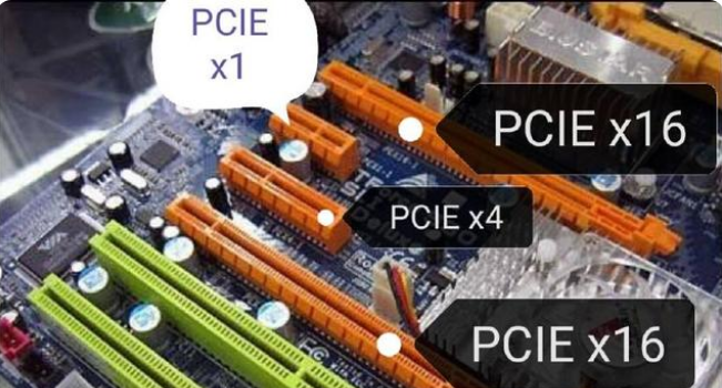
Interfaces and connectors: Examples include PCIe interfaces (for connecting to servers or computer motherboards), high-speed network interfaces (for multi-card interconnects or clusters), and various other I/O interfaces for communicating with external components like sensors and storage devices.
Power management module: Provides stable, efficient power supply to all components on the accelerator.
PCB Board Itself: Serves as the carrier for all components. AI accelerators, particularly those designed for data centers and high-performance computing, typically employ PCBs with high multilayer counts (even 20-30 layers or more) and HDI (High-Density Interconnect) processes. These PCBs utilize low-loss materials like Ultra Low Loss and require precise impedance control and crosstalk prevention to ensure the integrity and stability of high-speed signal transmission, while effectively managing thermal dissipation and power distribution.
The operating principle involves offloading computationally intensive AI tasks—such as image recognition, natural language processing, and video analysis—from the central processing unit (CPU) to dedicated AI accelerators. This leverages their parallel computing architecture to significantly enhance processing speed and energy efficiency.
Primary Forms and Installation Methods
AI accelerators with PCB assembly primarily come in three typical form factors and installation methods: The most common is as a PCIe expansion card, which can be directly inserted into the motherboard slot of a server or workstation, providing powerful AI computing power for general-purpose computing platforms; Second is the System-on-Module (SoM) form factor, integrating processors, memory, and multiple interfaces. This facilitates developers embedding it into custom baseboards or end devices, making it suitable for compact edge computing scenarios. Additionally, in certain highly integrated all-in-one devices, AI accelerator chips are directly integrated onto the motherboard as one of the core computing units. These form factors determine how accelerators connect and deploy within systems, spanning applications from data centers to embedded edge devices.
Application Scenarios
AI accelerators with PCB assembly find applications across diverse fields requiring efficient intelligent computing. Their core mission is to transform cloud-based AI algorithms into tangible intelligence deployable in the real world. In data centers and cloud computing, they are densely deployed within server clusters as PCIe accelerator cards, providing core computational power for large-scale machine learning model training and massive inference tasks. They serve as the foundational engines driving search engines, content recommendations, and cloud-based AI services like voice assistants and image generation. In autonomous driving, these accelerator modules are deeply integrated into vehicle computing platforms. They process continuous data streams from cameras, lidar, and millimeter-wave radar in real time, enabling complex environmental perception, high-precision positioning, path planning, and decision control—all demanding extreme real-time performance and reliability. In the realm of smart IoT and edge computing, these solutions typically take the form of highly integrated embedded core boards or modules deployed within smart security cameras, industrial quality inspection equipment, smart retail terminals, service robots, and industrial gateways. This enables devices to perform AI tasks like real-time image recognition, anomaly detection, and voice interaction at the data source, significantly reducing network latency and cloud dependency while enhancing data privacy protection. Furthermore, in scientific research (e.g., climate modeling, genetic sequence analysis), fintech (high-frequency trading, risk modeling, fraud detection), and medical imaging analysis, these systems significantly accelerate complex data processing and analysis through powerful parallel computing capabilities. They serve as the critical hardware foundation driving intelligent upgrades across industries.
Technical Challenges and Development Trends
The design and manufacturing of AI accelerator PCBs face high technical demands:High-density interconnects and thermal management: High component density and power consumption pose significant challenges for thermal design and PCB routing.
Signal integrity: High-speed signal transmission requires strict impedance control, minimized loss, and reduced crosstalk.
Reliability: Particularly in automotive electronics and similar fields, PCBs must operate stably under harsh conditions such as severe vibration and extreme temperature variations.
Trends include:Adopting more advanced PCB materials (e.g., M8/M9-grade high-frequency, high-speed copper-clad laminates) to reduce losses.
Process upgrades: Moving toward higher layer counts and more advanced HDI processes.
Increased integration: Tighter integration and coordination between accelerators and other computing units like CPUs and GPUs.
Specialization: Designing more dedicated accelerators tailored for specific AI workloads (e.g., Transformer models).
In simple terms, an AI accelerator with PCB assembly is a circuit board module that integrates dedicated AI processing chips, memory, interfaces, and other components, and has undergone assembly and packaging. It significantly boosts the processing speed of AI tasks through hardware acceleration. Its form factors vary widely, ranging from large PCIe accelerator cards for data centers to compact embedded core boards. It serves as the crucial hardware foundation driving the implementation of current artificial intelligence applications across diverse fields.
One-Stop HDI PCB Manufacturer and Its PCB Via Filing Capabilities
If you're looking for turnkey HDI electronics manufacturing services (EMS) from hardware development to PCBA fabrication and box-build assembly, you can work with the one-stop HDI PCBA manufacturer PCBONLINE.
Founded in 1999, PCBONLINE has R&D capabilities for HDI projects and EMS manufacturing capabilities, including via filling for stacked vias. It provides 4-to-64-layer HDI PCB fabrication, assembly, and PCBA box-build assembly. You can order various HDI PCBs from PCBONLINE, such as FR4, polyimide (flexible PCB), polyimide + FR4 (rigid-flex PCB), and PTFE/Rogers (high-frequency PCB).

3000m² of production capacity per day for HDI PCBs with builds of 1+N+1, 2+N+2, 3+N+3,4+N+4, and arbitrary interconnection in any layers.
PCBONLINE has hardware and software R&D capabilities for IoT applications requiring HDI design, including PCBA and enclosures.
We can manufacture complex PCBs with stacker vias, via-in-pad, microvias, inlay boards, heavy copper designs, and hybrid and fine structure lay-ups.
Besides HDI PCB fabrication, we have powerful capabilities in fine-pitch assembly for HDI PCB assembly.
We have rich R&D and manufacturing experience for HDI applications such as FPGA boards.
High-quality HDI PCB and PCBA manufacturing certified with ISO 9001:2015, IATF 16949, RoHS, REACH, UL, and IPC-A-610 Class 2/3.
Here'e the PCB via filing capabilities at PCBONLINEL:
- Micriavia filling with copper: laser via size 0.1-0.125mm, priority 0.1mm
- Finished hole size for via-in-pad filling with resin: 0.1-0.9mm (drill size 0.15-1.0mm), 0.3-0.55mm normal (drill size 0.4-0.65mm)
- Max aspect ratio for via-in-pad filling with resin PCB - 12: 1
- Min resin plugged PCB thickness: 0.2mm
- Max via-filling ith resin PCB thickness: 3.2mm
- Making different hole sizes with via filling in one board: Yes
- Via filling with copper/silver: Yes
If you need HDI PCBAs or any other PCBAs requiring via filling, please send your email to PCBONLINE at info@pcbonline.com. We will provide one-on-one engineering support to you.
Conclusion
Via filling is used for creating stacked vias in HDI PCB fabrication, BGA/CSP/QFN IC packaging, and filling PCB via-in-pad with resin during multilayer PCB fabrication. If you need one-stop electronics manufacturing for your HDI PCBA project, contact the one-stop advanced PCB manufacturer PCBONLINE for high-quality PCBA and box-build solutions tailored to your project's needs.
PCB fabrication at PCBONLINE.pdf


