
In today's exploding AI computing power, PCBs and PCBAs are no longer simply connection carriers; they have become core technologies that determine system performance and reliability. This article will delve into four key areas: board selection, high-density interconnection, solder joint inspection, and reliability assurance. It will also analyze how cutting-edge technologies can be used to create circuit solutions that meet the demands of the AI era.
In this article:
Part 1. Choosing the Right PCB Material for AI Signals Part 2. How to Achieve High-density Interconnection in Increasingly Smaller Spaces Part 3. Ensure Every Soldering Point is Perfect Part 4. Enabling AI Hardware to Run Stably in Extreme EnvironmentsChoosing the Right PCB Material for AI Signals
The performance bottleneck of AI hardware often begins with the fundamental PCB material. Traditional FR-4 material is like a congested road when faced with high-speed, high-frequency signals, resulting in severe signal loss and distortion. Therefore, selecting specialized materials with low dielectric constant (Dk) and low dissipation factor (Df), such as modified epoxy resin and polyimide, is crucial. These materials ensure smooth data transmission at speeds of 112 Gbps and above across the PCB. Furthermore, the enormous heat generated by AI chips places stringent demands on heat dissipation. We utilize highly thermally conductive metal substrates (such as aluminum silicon carbide (AlSiC)) and direct bond copper (DBC) technologies. These materials not only conduct heat quickly but also have a coefficient of thermal expansion (CTE) that matches the chip's performance, preventing cracking and failure caused by alternating hot and cold temperatures, thus ensuring product reliability and longevity from the very beginning.

How to Achieve High-density Interconnection in Increasingly Smaller Spaces
As electronic component sizes continue to shrink (e.g., 01005 specifications), PCB routing space has become extremely valuable. Using any-layer interconnect (HDI) technology, we drill tiny blind vias between all PCB layers, enabling complex routing similar to a three-dimensional transportation system, with line width/space accuracy exceeding 25 microns. This process relies on cutting-edge processes such as laser direct imaging (LDI) and semi-additive process (mSAP). Furthermore, advanced packaging technologies (such as embedded technology that embeds chips directly into the board or heterogeneous integration using silicon interposers for multi-chip interconnection) blur the line between PCB and chip, significantly shortening signal transmission paths and improving overall system integration and computing speed.

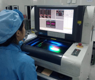
Ensure Every Soldering Point is Perfect
With components so small they're indistinguishable to the naked eye, ensuring the quality of tens of thousands of solder joints presents a significant challenge. We rely on a deep learning-based automated optical inspection (AOI) system, which acts like a "smart quality inspector," automatically identifying defects such as cold solder joints and bridging with over 99.5% accuracy. For solder joints hidden beneath the chip, such as those on BGAs and completely invisible to the naked eye, we must employ fluoroscopic inspections using microfocus X-rays and computed tomography (CT) scanners. These machines can quantify the void rate within the solder joints with micron-level accuracy, ensuring the absence of any hidden defects. For soldering materials, we use Type 4/5 ultra-fine solder paste and high-performance underfill, which effectively absorbs stress and protects the tiny solder joints from fatigue fracture in harsh environments.
Enabling AI Hardware to Run Stably in Extreme Environments
Qualified AI hardware must withstand long-term, high-load operation. We verify product durability through accelerated life testing (ALT) by simulating years or even longer of extreme operating conditions in our labs. This includes severe temperature cycling (-55°C to 125°C), high temperature and humidity (85°C/85% RH), and continuous vibration. To address the critical heat dissipation issue, we go beyond traditional heat sinks and employ high-efficiency thermal interface materials (TIMs) such as thermally conductive gels and phase change materials. We also incorporate advanced solutions such as vapor chambers and direct liquid cooling to quickly dissipate the enormous heat generated by the chip, preventing it from throttling or damage due to excessive heat. Finally, any potential failures are traced to their root causes through microscopic analysis methods such as scanning electron microscopy (SEM), forming a closed-loop quality improvement loop from design to manufacturing to ensure the robustness and reliability of every delivered board.

Amidst the rapid evolution of AI hardware, excellent PCB/PCBA design and manufacturing are no longer just supporting elements; they are now the defining factors for product success. From materials science to manufacturing processes, from testing technology to reliability engineering, advancements in every aspect are paving the way for unleashing AI computing power. Only by mastering these core technologies can we build the hardware foundation for true competitiveness in this technological revolution.
One-Stop HDI PCB Manufacturer and Its PCB Via Filing Capabilities
If you're looking for turnkey HDI electronics manufacturing services (EMS) from hardware development to PCBA fabrication and box-build assembly, you can work with the one-stop HDI PCBA manufacturer PCBONLINE.
Founded in 1999, PCBONLINE has R&D capabilities for HDI projects and EMS manufacturing capabilities, including via filling for stacked vias. It provides 4-to-64-layer HDI PCB fabrication, assembly, and PCBA box-build assembly. You can order various HDI PCBs from PCBONLINE, such as FR4, polyimide (flexible PCB), polyimide + FR4 (rigid-flex PCB), and PTFE/Rogers (high-frequency PCB).

3000m² of production capacity per day for HDI PCBs with builds of 1+N+1, 2+N+2, 3+N+3,4+N+4, and arbitrary interconnection in any layers.
PCBONLINE has hardware and software R&D capabilities for IoT applications requiring HDI design, including PCBA and enclosures.
We can manufacture complex PCBs with stacker vias, via-in-pad, microvias, inlay boards, heavy copper designs, and hybrid and fine structure lay-ups.
Besides HDI PCB fabrication, we have powerful capabilities in fine-pitch assembly for HDI PCB assembly.
We have rich R&D and manufacturing experience for HDI applications such as FPGA boards.
High-quality HDI PCB and PCBA manufacturing certified with ISO 9001:2015, IATF 16949, RoHS, REACH, UL, and IPC-A-610 Class 2/3.
Here'e the PCB via filing capabilities at PCBONLINEL:
- Micriavia filling with copper: laser via size 0.1-0.125mm, priority 0.1mm
- Finished hole size for via-in-pad filling with resin: 0.1-0.9mm (drill size 0.15-1.0mm), 0.3-0.55mm normal (drill size 0.4-0.65mm)
- Max aspect ratio for via-in-pad filling with resin PCB - 12: 1
- Min resin plugged PCB thickness: 0.2mm
- Max via-filling ith resin PCB thickness: 3.2mm
- Making different hole sizes with via filling in one board: Yes
- Via filling with copper/silver: Yes
If you need HDI PCBAs or any other PCBAs requiring via filling, please send your email to PCBONLINE at info@pcbonline.com. We will provide one-on-one engineering support to you.
Conclusion
Via filling is used for creating stacked vias in HDI PCB fabrication, BGA/CSP/QFN IC packaging, and filling PCB via-in-pad with resin during multilayer PCB fabrication. If you need one-stop electronics manufacturing for your HDI PCBA project, contact the one-stop advanced PCB manufacturer PCBONLINE for high-quality PCBA and box-build solutions tailored to your project's needs.
PCB fabrication at PCBONLINE.pdf


