
With the deep integration of artificial intelligence and medical technology, medical robots are undergoing a profound transformation driven by underlying hardware. This transformation goes beyond a simple performance upgrade; it encompasses a comprehensive paradigm shift in perception, computing, storage, and integration. From perception systems that emulate the synergy of human multi-sensory systems, to distributed and embedded intelligent decision-making cores, to efficient storage interconnects and advanced packaging technologies designed to handle massive amounts of data, the coordinated evolution of these hardware components is shaping the future of next-generation medical robots: more precise, safer, and more autonomous. This article will delve into these four core hardware development trends and reveal how they are infusing AI medical robots with true soul.
In this article:
Part 1. Powerful Perception System Part 2. Intelligent Computing and Control Part 3. Efficient Storage and Interconnection Part 4. Advanced Packaging and IntegrationPowerful Perception System
Multi-sensor fusion is evolving from single-mode perception to multimodal collaborative perception. Modern AI medical robots are no longer content with acquiring image information solely through visual cameras. They are increasingly integrating high-precision six-dimensional force/torque sensors, inertial measurement units (IMUs), and cutting-edge flexible electronic skin to simulate human tactile perception. This multi-sensor data fusion technology enables robots to "feel" the magnitude and direction of force acting on the end of instruments in real time when performing delicate tasks such as suturing or tissue removal, enabling precise closed-loop control of operating force, significantly improving surgical safety and accuracy.
In the field of imaging and simulation, perception systems are evolving from providing basic images to providing computable depth perception data. In addition to advances in hardware sensors, GPU-accelerated ultrasound simulation technology can generate realistic synthetic ultrasound images, providing AI models with massive and diverse training data. This means that the robot's vision system has been "trained" millions of times in highly realistic virtual environments before it is put into use. This simulation-driven perception training, combined with real-time 4K/8K ultra-high-definition endoscopic images during surgery, jointly builds a complete perception closed loop from preoperative simulation to real-time navigation during surgery, significantly enhancing the robot's environmental understanding and decision-making capabilities.
Intelligent Computing and Control
In computing architecture, centralized processing is being replaced by distributed collaborative computing. To meet the stringent real-time requirements of complex tasks, AI medical robots generally adopt a layered, distributed control architecture. Within this architecture, high-level decision-making, mid-level sensor fusion, and low-level motor servo control are distributed to separate dedicated processors, achieving functional decoupling and parallel processing. This not only effectively reduces the processing load on a single core, ensuring timely system response, but also greatly enhances the modularity and maintainability of the hardware system, facilitating future upgrades and functional expansion.
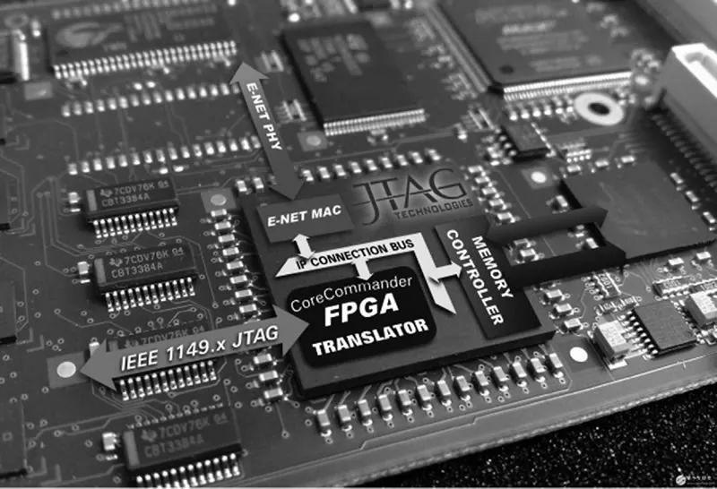
Artificial intelligence has evolved from a cloud-based auxiliary tool to a real-time decision-making core embedded in the hardware itself. This is marked by the deep integration of dedicated AI processing units (such as NPUs) and FPGAs. The NPU provides robots with powerful local AI computing power, enabling them to perform real-time vision tasks such as semantic segmentation of endoscopic images and instrument tracking without relying on the cloud. The FPGA, with its reconfigurable hardware, provides hardware acceleration for specific sensor interface protocols and pre-processing algorithms, achieving ultra-low latency in the microsecond range. This "sinking of computing power" to the edge is key to ensuring the real-time operation and data security of medical robots.
Efficient Storage and Interconnection
The data storage paradigm is shifting from a processor-centric to a data-centric one. Faced with the massive amounts of high-resolution video streams and sensor data generated during surgery, traditional memory architectures face significant power consumption and latency bottlenecks due to frequent data movement. To address this, emerging architectures such as in-memory computing have emerged. By performing computations directly within the memory unit, they significantly reduce data movement. This approach is particularly well-suited for the frequently invoked AI algorithm models in medical robots, resulting in orders of magnitude improvements in computing energy efficiency and speed.
The bandwidth of hardware interconnect interfaces is undergoing a revolutionary improvement. Efficient collaboration between various computing units within a robot (such as the CPU, GPU, and FPGA) and sensors relies heavily on high-speed interconnect buses. High-speed serial bus standards such as PCIe 5.0/6.0 offer unprecedented data transfer rates, ensuring smooth transmission of images with resolutions exceeding 4K and instantaneous response to control commands. When multiple AI chips are working together, point-to-point high-speed interconnect technologies such as NVLink eliminate traditional bus bottlenecks, establishing a full-bandwidth, low-latency "data highway" between chips and fully unleashing the potential of distributed computing clusters.

Advanced Packaging and Integration
Chip-level integration technology has evolved from two-dimensional to three-dimensional, giving rise to more powerful and compact "superchips." As transistor scaling approaches physical limits, multi-chiplet design and 2.5D/3D advanced packaging technologies are crucial for sustaining Moore's Law. By integrating multiple small chips with different processes and functions (such as CPUs, I/O devices, and AI accelerators) in a three-dimensional stack within a single package, this approach achieves the performance and efficiency of a single chip while offering the flexibility and low-cost advantages of modular design. This allows medical robot main control chips to maintain miniaturization while doubling their integration density and computing power.
Board-level and system-level integration place greater emphasis on signal integrity and electromagnetic compatibility. When data transmission speeds within a chip reach tens of Gb/s, traditional PCB materials and designs can no longer guarantee signal quality. Therefore, high-speed materials with low dielectric loss factor (Df), such as modified polyphenylene ether (PPO), are an inevitable choice. These new materials can effectively reduce signal loss and distortion during transmission, ensuring stable and reliable data communication between the processor, memory, and sensors, and guaranteeing the stable operation of the entire medical robot hardware platform in complex electromagnetic environments from the bottom of the system.

In summary, the development trajectory of AI medical robot hardware clearly points toward a higher level of integration, intelligence, and collaboration. The multimodal fusion of perception systems gives robots "super senses" that surpass those of humans. Distributed computing and embedded AI empower them with a "edge brain" capable of real-time decision-making. Revolutionary storage, interconnection, and packaging technologies build an efficient and reliable "neural network and skeleton." These trends do not exist in isolation; rather, they are intertwined and mutually reinforcing, collectively driving the evolution of medical robots from sophisticated auxiliary tools to intelligent partners capable of deeply understanding their environment and autonomously performing complex tasks. In the future, with continued breakthroughs and cost optimization in these hardware technologies, high-level robot-assisted diagnosis and treatment are expected to expand beyond top hospitals into a wider range of applications, ultimately reshaping the global healthcare landscape.
One-Stop HDI PCB Manufacturer and Its PCB Via Filing Capabilities
If you're looking for turnkey HDI electronics manufacturing services (EMS) from hardware development to PCBA fabrication and box-build assembly, you can work with the one-stop HDI PCBA manufacturer PCBONLINE.
Founded in 1999, PCBONLINE has R&D capabilities for HDI projects and EMS manufacturing capabilities, including via filling for stacked vias. It provides 4-to-64-layer HDI PCB fabrication, assembly, and PCBA box-build assembly. You can order various HDI PCBs from PCBONLINE, such as FR4, polyimide (flexible PCB), polyimide + FR4 (rigid-flex PCB), and PTFE/Rogers (high-frequency PCB).

3000m² of production capacity per day for HDI PCBs with builds of 1+N+1, 2+N+2, 3+N+3,4+N+4, and arbitrary interconnection in any layers.
PCBONLINE has hardware and software R&D capabilities for IoT applications requiring HDI design, including PCBA and enclosures.
We can manufacture complex PCBs with stacker vias, via-in-pad, microvias, inlay boards, heavy copper designs, and hybrid and fine structure lay-ups.
Besides HDI PCB fabrication, we have powerful capabilities in fine-pitch assembly for HDI PCB assembly.
We have rich R&D and manufacturing experience for HDI applications such as FPGA boards.
High-quality HDI PCB and PCBA manufacturing certified with ISO 9001:2015, IATF 16949, RoHS, REACH, UL, and IPC-A-610 Class 2/3.
Here'e the PCB via filing capabilities at PCBONLINEL:
- Micriavia filling with copper: laser via size 0.1-0.125mm, priority 0.1mm
- Finished hole size for via-in-pad filling with resin: 0.1-0.9mm (drill size 0.15-1.0mm), 0.3-0.55mm normal (drill size 0.4-0.65mm)
- Max aspect ratio for via-in-pad filling with resin PCB - 12: 1
- Min resin plugged PCB thickness: 0.2mm
- Max via-filling ith resin PCB thickness: 3.2mm
- Making different hole sizes with via filling in one board: Yes
- Via filling with copper/silver: Yes
If you need HDI PCBAs or any other PCBAs requiring via filling, please send your email to PCBONLINE at info@pcbonline.com. We will provide one-on-one engineering support to you.
Conclusion
Via filling is used for creating stacked vias in HDI PCB fabrication, BGA/CSP/QFN IC packaging, and filling PCB via-in-pad with resin during multilayer PCB fabrication. If you need one-stop electronics manufacturing for your HDI PCBA project, contact the one-stop advanced PCB manufacturer PCBONLINE for high-quality PCBA and box-build solutions tailored to your project's needs.
PCB fabrication at PCBONLINE.pdf


