
In very simple words PCB is a short form of "Printed Circuit Board". It comes with a couple of names. Most often, we call it PCB, or PCB board too.
In this blog, we will go over the PCB meaning, functions of PCB, and other things related to PCBs.
What Does PCB Stand for?
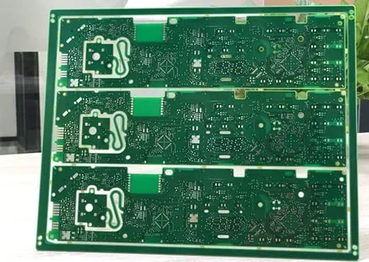
PCB is a short form with several meanings. What does PCB mean in electronics? In electronic fields, PCB stands for printed circuit board, which is a mainboard supporting and connecting electronic components.
![]()
Whether you are an electrical engineer, student, or researcher in electronics, you need to deal with PCB and related products every day, such as PCB layout, components, and product R&D. So understanding the PCB meaning is one of the most basic things for you.
Essentially, a PCB is a system of conductive patterns located in the volume and on the surface of a dielectric base, interconnected by the circuit diagram.
Many types of PCBs are very different. However, the normal PCB structure includes a substrate, alternating layers of prepreg and copper traces, copper pads on the surface, copper vias connecting different PCB layers, and solder masks.
In a PCB, the copper vias connect copper traces in different layers, and the PCB pads on the surface of the dielectric base are designed to solder to connect electronic components. In this manageable way, various components can integrate on a tiny PCB board and connect.
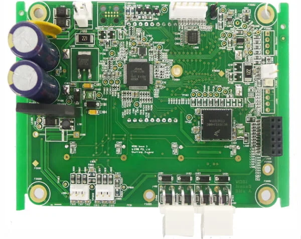
Now you can understand what PCB stands for in electronics. As the carrier of electronic components and provides electrical connection, PCB is a basic and critical component for all modern electronic devices and systems.
With the advent and incremental development of PCBs, the volume of electronic products gets smaller and smaller (imagine the earliest computer as large as a classroom and a palm-sized microcomputer nowadays), and the electrical functions of electronic devices are more and more.
How does PCB benefit the progress of electronics? Just see the functions of PCBs below.
PCB Functions
Circuit boards are used for electrical connection and mechanical fastening of quantum electronics and electronic components - passive and active electronic components installed on them.
The role of the PCB is to support the electronic components and to ensure the electrical connections necessary for the operation of the system. PCB cannot perform these functions alone, soldering is necessary to make the mechanical and electrical connections between the components and the tracks of the circuit.
Functions of PCBs include:
- Mechanical support: All PCBs can mount electronic components and provide mechanical support to them. A rigid PCB has good mechanical strength and is the supporting framework of the electronic device.
- Electrical connection: PCB establishes electrical connections for components by providing a network of copper traces. The traces carry power and signals between different parts of a circuit to enable communication and functionality.
- Thermal dissipation: PCB plays an important role in thermal dissipation to protect components and the circuit from overheating. A PCB can not only mount a heat sink to dissipate thermal, but also the PCB itself can dissipate heat, especially ceramic PCBs and MCPCBs.
- Miniaturization of device volume and weight: The use of PCB makes various components integrate on a tiny board and saves the space and weight of an electronic product. With microvias and multiple circuit layers, you can make the product space smaller.
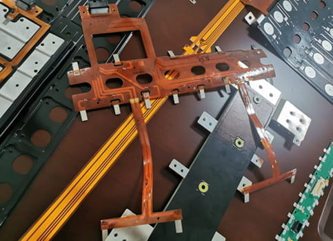
- Flexibility: By using flexible PCB materials such as polyimide (PI) or polyester (PET), a flexible PCB can bend, stretch, and shrink to fit a compact space. Besides, the use of flexible PCBs saves connectors. They are thin and further minimize the product size.
- Improving RF signal transmission and reception: In a PCB, it is the copper traces that carry signals and are responsible for signal transmission. However, for high-speed and high-frequency circuits, the PCB material is critical, and the functions of PCB include improving radio-frequency (RF) signal receiving and transmission. Using the PTFE material, a high-frequency PCB features excellent dielectric properties and a small coefficient of expansion and contraction, facilitating the RF signal distribution.
From calculators and microwave ovens to cell phones and aircraft control systems, all electronic equipment used today involves the use of PCBs. The purpose of printed circuit boards is, in a simplified way, to connect electrical components in an organized manner.
To successfully achieve PCB functions, the circuit must exercise, and you need to make sure to work with a reliable PCB manufacturer.
Where to Get PCB Printed - PCBONLINE
PCBONLINE is a one-stop PCB manufacturer for all types of PCBs, especially for advanced PCBs. Founded in 1999, it is an ISO-certified electronic contract manufacturer for middle and high-end electronic applications.
Whether you are an original equipment manufacturer (OEM), electrical engineer, business maker, or researcher in an institute, you can get PCBs made and assembled from PCBONLINE.
By working with PCBONLINE, you can enjoy below benefits:
- Any PCBs can be manufactured and assembled from PCBONLINE from prototypes to massive production.
- One-on-one engineering support and PCB design optimization from professional CAM and PCBA engineers.
- High-quality PCB, components, and PCBA certified with ISO 9001:2015, IATF 16949, RoHS, REACH, IPC, and UL.
- Affordable PCBs and PCBA because PCBONLINE has two PCB manufacturing bases and one PCB assembly factory. And relying on the EMS PCBA factory, PCBONLINE can buy original components with discounts.
- PCBONLINE can take part in R&D with you from the early developing stage. With an optimum PCB design, the fabrication price of your project can be reduced without functional or quality sacrifice.
With 24 years of PCB fabrication and assembly experience, PCBONLINE has many successful cases in consumer electronics and industrial, automotive, aerospace, military, computing, communication, biological, and agricultural applications. You can send your Gerber or any inquiry to info@pcbonline.com for a quote.
The Connection between PCB, Electric Circuit Diagram, and Electronic Components
Planning is the keyword that defines PCB fabrication since its entire creation process is methodical. There is an exchange of debugging and troubleshooting of your circuit for the previous logical organization of its components.
That is, it is necessary to think very carefully about the connections and functions of each of the elements of your circuit before making it, with this, it is possible to not have problems of bad contact in the wiring.
The wiring diagram and the netlistWhether it is made with Cadence OrCAD or with Mentor DxD, the electrical designer proceeds to study the electrical functionality to be created.
Once all the necessary components have been identified, the list of components (BOM, Bill Of Material) is drawn up for the purchase of the same.
The drafting of the electrical circuit diagram takes place at the same time as the BOM; first place the electrical symbols and then connect through the so-called "net".
Once the wiring diagram is frozen, the "netlist" is exported, and a table representing the electrical connections present and the components used.
The placement of components
Once the netlist is exported, it is imported into the routing software which translates each line of code into connections with all the indications of the components present.
Positioning is one of the most critical phases of the Master PCB because the choice and positioning criteria adopted for the components will influence the routing of the tracks.
A good positioning at this stage will avoid many problems of interference, crosstalk, and coupling of critical signals.
The positioning of the components will always be carried out taking into account the electrical functions of the parts, avoiding the no-go areas for placement and the routing of the tracks.
Track routing is the interconnection of all the connections present in the wiring diagram between the components.
The tracks that will be created will connect the pin pads of the components and will use multiple interconnection layers to concentrate all the connections inside the PCB.
Each layer is interconnected by metalized holes, also called vias.
The size of the tracks will be suitably calibrated according to the electrical constraints of the signals that will cross the board.
All electrical insulation (track-track, track-pitch, pitch-pitch, track-floor, floor-via, track-away, pitch-away, etc.) must be carefully chosen.
Impedance control, crosstalk, and signal IntegritySpecial attention should be given to impedance control and relative adaptation so that the condition of maximum power transfer between the generator and the user is always reached.
During routing it is essential to pay attention to critical signals and treat them properly right away, avoiding crosstalk or crosstalk problems because it is the electromagnetic field that is generated in a track when current flows, generating an exchange of energy from one track to another.
This creates an undesirable disturbance due to the induced spurious current which affects the quality of the signals and results in a reduction in communication speed.
A good digital signal has fast transitions and logic levels that are clean and free of transient phenomena.
The circuit diagram is a diagram showing circuit connections within a code of a circuit element.
Schematics is a type of schematic layout of components and their relationships drawn with physically and electrically standardized symbols for research and technical planning.
Schematics can convey the working principles of components, analyze their performance, and provide a planning system for installing electronic and electrical products.
In the circuit design, the technician can settle on paper or a computer after confirming that the actual installation is complete.
Improve, fix, and succeed through debugging.
Using circuit simulation software for circuit-assisted design and virtual circuit experiments can improve the work efficiency of engineers, save learning time, and make real pictures more intuitive.
Parts in the circuit do not necessarily resemble or are completely different in shape from the actual parts.
However, it generally represents the characteristics of the element, and the number of pins matches the actual element.
Like many wires in radio schematics, they are not necessarily straight in the printed circuit board diagram, but they can also be copper films of a particular shape.
A node represents a connection between multiple pins or wires.
All pins and conductors of the components connected to the node are conductive, no matter how many.
Annotations are significant in schematics and all text in the schematic can be categorized as annotations.
If you look closely at the figure above, you can see that there are annotations in various parts of the schematic. Annotations indicate the type, name, etc. of a component.
PCB Drawing Software
Since the official birth of commercial CAD systems (EDA), various design software has been developed since 1981. Printed circuit boards are the backbone of any hardware product. Before the development of EDA software, engineers typically designed electronic circuits and integrated circuits by hand or in some other non-automated way.
Autodesk Eagle
![]()
Eagle is perhaps one of the most famous programs for designing circuits and printed circuit boards. Formerly known as Cadsoft Eagle, this software suite is now called Autodesk Eagle following its purchase by Autodesk. Autodesk EAGLE contains a schematic editor for schematic diagram design and a PCB layout editor for designing printed circuit boards. It provides component placement, PCB routing, extensive library content, a thriving community, and more. You can also find a free version of Autodesk EAGLE. It is available for Windows, Linux, and Mac.
Expresspcb Plus
![]()
ExpressPCB Plus is CAD software for electronic circuit creation and design. It includes ExpressSCH Classic for schematic drawing and Express PCB Plus for PCB design. ExpressPCB Plus provides the ability to see the current development prices for your board, and even order a board to manufacture from within the program itself. ExpressPCB is available for use on Windows, Linux, and Mac.
Features of PCB Design for STM32WB
Microwave tracing of printed circuit boards must be carefully worked out. Let's consider the main aspects of PCB design for STM32WB. Let's start with impedance matching.
It is known that to reduce signal reflection it is necessary to match the impedance of the source, receiver, and transmission line.
The impedance of a transmission line depends on its geometry and the location of the supporting surface. By the reference surface, I mean a conductive layer with zero potential, the geometrical dimensions of which significantly exceed the dimensions of the conductive line.
Let's list the main factors influencing the wave impedance of the transmission line:
- Line type: microstrip, strip, coplanar
- Line width
- Distance to the support layer H (dielectric thickness).
- Dielectric material parameters (dielectric constant)
- The thickness of the conductive layer, which is more influenced by the thickness of the conductor T1, to a lesser extent by the thickness of the copper of the reference layer T2;
- Solder mask thickness
The impedance of a transmission line depends on its geometry and the selected PCB layer stack. Depending on whether the priority is stack or geometry, there are two approaches to design.
The first approach is that the developer of the board sets the geometric dimensions of the conductors convenient for him, and then selects the layer stack and production technology for them. However, it is far from always possible to find the required stack within the technological limitations of the PCB manufacturer.
A situation may arise in which even if the manufacturer can produce a board on a given stack, its cost will be much higher than the typical one, especially when it comes to a small series or a prototype. Another approach is to select a generic stack from the manufacturer.
Each PCB manufacturer has recommended solutions, the use of which ensures the minimum production cost. But in this case, you will have to select the geometry of the transmission lines for the available parameters, and this does not always suit the developer. Both approaches require the developer to work closely with the manufacturer.
Conclusion
This article defines PCB meaning and introduces related things such as PCB functions, where to get PCBs made, and PCB design. To get high-quality and affordable PCBs, you can work with a source factory PCB manufacturer PCBONLINE, from where you will get satisfying services and products.


