
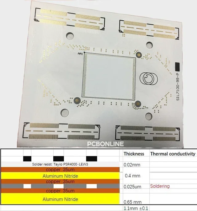
A ceramic PCB is a printed circuit board using ceramics as the substrate materials, such as aluminum oxide, aluminum nitride, silicon nitride, etc. The ceramic PCB's conductive layers are bonded on the ceramic substrate by magnetron sputtering. A ceramic PCB assembled with LEDs as below is used for the spotlight.
![]()
What is a Ceramic PCB?
Ceramic PCBs use ceramics as their base materials, and they require much higher manufacturing temperatures than other PCBs. As PCB base materials, ceramics used for PCBs have the advantages of both FR4 and metal. FR4 materials are electrically insulating, but their thermal conductivity is poor; aluminum and copper have excellent thermal conductivity, but they are conductors. Ceramic PCBs have good thermal conductivity and do not require an electrical insulation layer as ceramics are good insulators.
When ceramic PCBs are mounted with LED chips, ICs, and other components, they become ceramic PCBAs. LEDs can be assembled on the ceramic PCBs by wire bonding or flip-chip method. Ceramic PCBAs are usually the core parts in high-power and high-frequency applications, such as car-scale power controllers, variable optical systems, exchange converters, solar power batteries, high-current LED lights, etc...
What is A Ceramic PCB's Structure?
A single-layer ceramic PCB consists of a ceramic substrate layer, a copper layer, and a solder mask layer. We will discuss the double-layer ceramic PCBs' structure to help you better understand what a ceramic PCB is.
Below is the structure of a single-sided double-layer ceramic PCB manufactured with the normal lamination method.
![]()
1. Ceramic substrate:
Unlike aluminum or FR4, ceramic has both good thermal conductivity and electrical insulation. So ceramic substrate plays two roles, one for thermal dissipation, and the other for insulation between the circuit layers. For double-layer and multilayer ceramic PCBs, PCB holes are necessary, and the vias are drilled by laser in the ceramic substrate. Then the PCB vias are filled with copper plating.
2. Copper layer:
A copper layer is a thin copper foil. It is bonded to the ceramic substrate by magnetron sputtering. When the copper foil is bonded to the ceramic substrate, the circuit is etched on the copper foil with the photoresist coating of the yellow light method.
3. Dielectric layer (PP):
PP can be phenolic, epoxy resin, special thermal conductive materials, etc. The dielectric layer is used to bond the two adjacent ceramic substrate boards. However, PP has worse thermal conductivity than ceramics and reduces the overall thermal conductivity of the ceramic PCB. So a ceramic PCB with a dielectric layer is used for applications with lower thermal dissipation requirements.
4. Solder mask:
Solder masks protect the exposed copper wires from solder, metals, and damage from the environment. After the PCB is laminated, a solder mask is applied above the circuit layer. The color of the solder mask can be green, white, beige, etc.
Below is the structure of a single-sided double-layer ceramic PCB manufactured with the sintering lamination method.
![]()
The ceramic substrate layers, copper layers, and solder masks are the same as the above. But it doesn't have a dielectric layer. This is because the two ceramic substrate boards are directly bonded without PP. At higher sintering temperatures, molecules of two attached surfaces migrate to each other sides and form dense polycrystalline ceramics. There is more reliability of the bonding between copper and ceramics in this way. The thermal conductivity of the ceramic PCB is much higher than the above ceramic PCB's.
What is Unique about Ceramic PCB: Ceramic PCB vs. Normal PCB
A ceramic PCB is unique because of the ceramic PCB materials and improved performance. First, let's compare the PCB materials of ceramic PCBs and normal PCBs.
|
|
Ceramic PCB
|
Normal PCB
|
|
Base Substrates
Base Substrates
|
Aluminum oxide (alumina)
Aluminum nitride (AlN)
Silicon nitride
Carbon carbide
Boron oxide (poisonous)
|
Glass fiber/FR4
Phenolic resin/FR3
Aluminum
Copper
Composite ceramics
|
|
Adhesive
|
PP (normal lamination)
None (sintering lamination)
|
Phenolic
Epoxy
|
|
Conductive Layers
|
Copper
|
Copper
|
The main difference between ceramic PCBs and normal PCBs is the ceramic base material. So what are the improved characteristics of ceramic PCBs?
|
|
Ceramic PCB
|
Normal PCB (aluminum)
|
|
Thermal conductivity
|
Alumina: 15 to 35W/(m·K)
AlN: 170 to 260W/(m·K)
|
1 to 9W/(m·K)
|
|
Need an insulation layer?
|
No
|
Yes
|
|
Thermal Expansion Coefficient
|
Alumina: 6 to 10×10ˆ(-6)°C
AlN: 4.6×10ˆ(-6)°C
|
50×10ˆ(-6)°C
|
|
Dielectric Constant
|
Alumina: 9 to 10
AlN: 10
|
/
|
|
Dielectric Loss
|
Alumina: 1 to 5×10ˆ(-4)
AlN: 3.8×10ˆ(-4)
|
/
|
Compared with normal PCBs, ceramic PCBs have a higher mechanical strength, smaller warpage, higher thermal shock resistance, smaller DK/Df, higher thermal conductivity, closer thermal expansion coefficient with silicon, better chemical stability, and no water absorption.
Besides carrying components, a ceramic PCB can be three-dimensional and function as a support component for modules.
Types of Ceramic PCBs
Based on the classification of ceramic substrates, ceramic PCBs are classified as:
- Alumina PCBs (Al₂O₃): Alumina PCBs are the most used ceramic PCBs. Aluminum oxide is also the cheapest ceramic PCB substrate.
- Aluminum nitride PCBs (AlN): Aluminum nitride PCBs are also commonly used ceramic PCBs and are more expensive than alumina PCBs. AlN has better thermal conductivity and high-frequency performances than alumina.
- Silicon nitride PCBs (Si₃N₄): Si₃N₄ has higher costs than AlN. Silicon nitride PCBs feature high mechanical strength and toughness, and they are mainly used for power electronic modules, such as IGBT modules, car-scale modules, and military/aerospace/aviation modules.
- Silicon carbide PCBs (SiC): silicon carbide is diamond. It has high thermal conductivity. As an electrical semiconductor, SiC has high conductivity. Silicon carbide PCBs are mainly used in laser fields.
- Boron oxide PCBs (BeO): BeO has a dozen times more thermal conductivity than alumina, but it is poisonous. BeO PCBs have low DK and Df, and they are used for high-frequency and high-power applications.
Based on the classification of manufacturing methods, ceramic PCBs are classified as:
- HTCC ceramic PCBs: HTCC stands for high-temperature co-fired ceramic and is the earliest ceramic PCB manufacturing method. HTCC ceramic PCBs are suitable for high-power but not high-frequency/high-speed applications.
- DBC ceramic PCBs: DBC stands for direct bonding copper, and it requires lower temperatures than HTCC. DBC ceramic PCBs have no PTH vias. They are mainly used for packaging for power electronic modules, LED devices, etc.
- Thick film ceramic PCBs: Thick film ceramic PCBs require the circuit line space to be at least 60μm. However, the circuit of thick film ceramic PCBs is of high precision. They are mainly used for applications having lower requirements for power.
- LTCC ceramic PCBs: LTCC stands for low-temperature co-fired ceramic. LTCC ceramic PCBs are usually multilayer and three-dimensional. LTCC ceramic PCBs are especially suitable for high-frequency communication devices.
- Thin-film ceramic PCBs: The circuit of thin-film ceramic PCBs is of high precision. However, there is a limit to the copper thickness of the circuit layer. Thin-film ceramic PCBs are suitable for high-precision packaging and devices in a small size.
- DPC ceramic PCBs: DPC stands for direct plating copper and develops from thin-film technology. DPC ceramic PCBs can be three-dimensional and have circuits of high precision. They are used for high-power and high-frequency applications.
Quality Ceramic PCB Manufacturer - PCBONLINE
Leading Ceramic PCB manufacturer PCBONLINEmanufactures and assembles the above ceramic PCBs except for the poisonous BeO PCBs. If you are seeking ceramic PCB manufacturing, PCBONLINE is one of the best ceramic PCB manufacturers because:
- PCBONLINE adopts the DPC technology to manufacture ceramic PCBs and can achieve 3D designs.
- PCBONLINE can manufacture ceramic PCBs to be HDI, high-frequency, multilayer, and double-sided.
- The copper layer thickness of ceramic PCBs is arbitrarily custom from 1μm to 1mm.
- Ceramic PCBs have no oxide layer on the PCB surface and have better welding performance and temperature resistance.
- PCBONLINE provides one-on-one engineering support and DFX to ceramic PCB projects.
PCBONLINE provides online ceramic PCB quotes. Register, and you will receive $100 coupons for online purchases. For ceramic PCB manufacturing and assembly orders at $5,000 and above, we provide complete ceramic PCBA samples, functional tests, and discounts.
Conclusion
This article introduces what a ceramic PCB is, the ceramic PCB structure, its features, and its types. For their three-dimensional design, ceramic PCBs not only load and connect components for high-power devices and packaging but mechanically support modules. This article also recommends a reliable ceramic PCB manufacturer for senior engineers, solutions companies, research institutes, and business makers. If you are seeking ceramic PCB manufacturing and assembly, PCBONLINE is one of your best ceramic PCB suppliers.


